Large substrate test system

a test system and large substrate technology, applied in the field of electromechanical test systems for large substrates, can solve the problems of increased shipping costs, large equipment size, and high ownership costs

Inactive Publication Date: 2006-02-02
APPLIED MATERIALS INC
View PDF51 Cites 16 Cited by
  • Summary
  • Abstract
  • Description
  • Claims
  • Application Information

AI Technical Summary

Problems solved by technology

Larger equipment requires more space, i.e., a larger footprint per processing unit throughput, resulting in a higher cost of ownership.
The large size of the equipment also increases the costs associated with shipping and may, in some cases, restrict the means and locales to which such equipment may be transported.

Method used


Image

  • Large substrate test system
  • Large substrate test system
  • Large substrate test system

Examples


Embodiment Construction

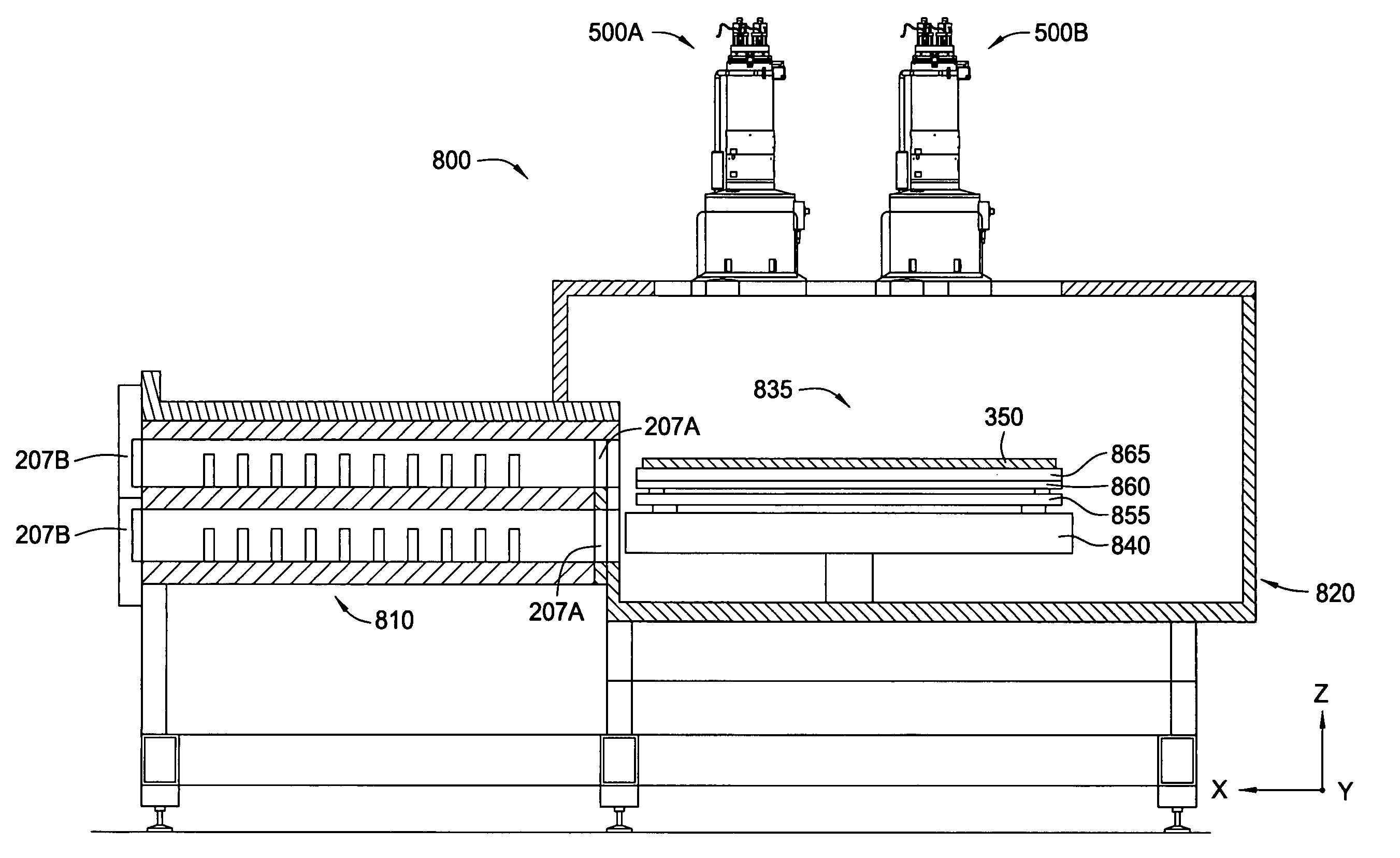
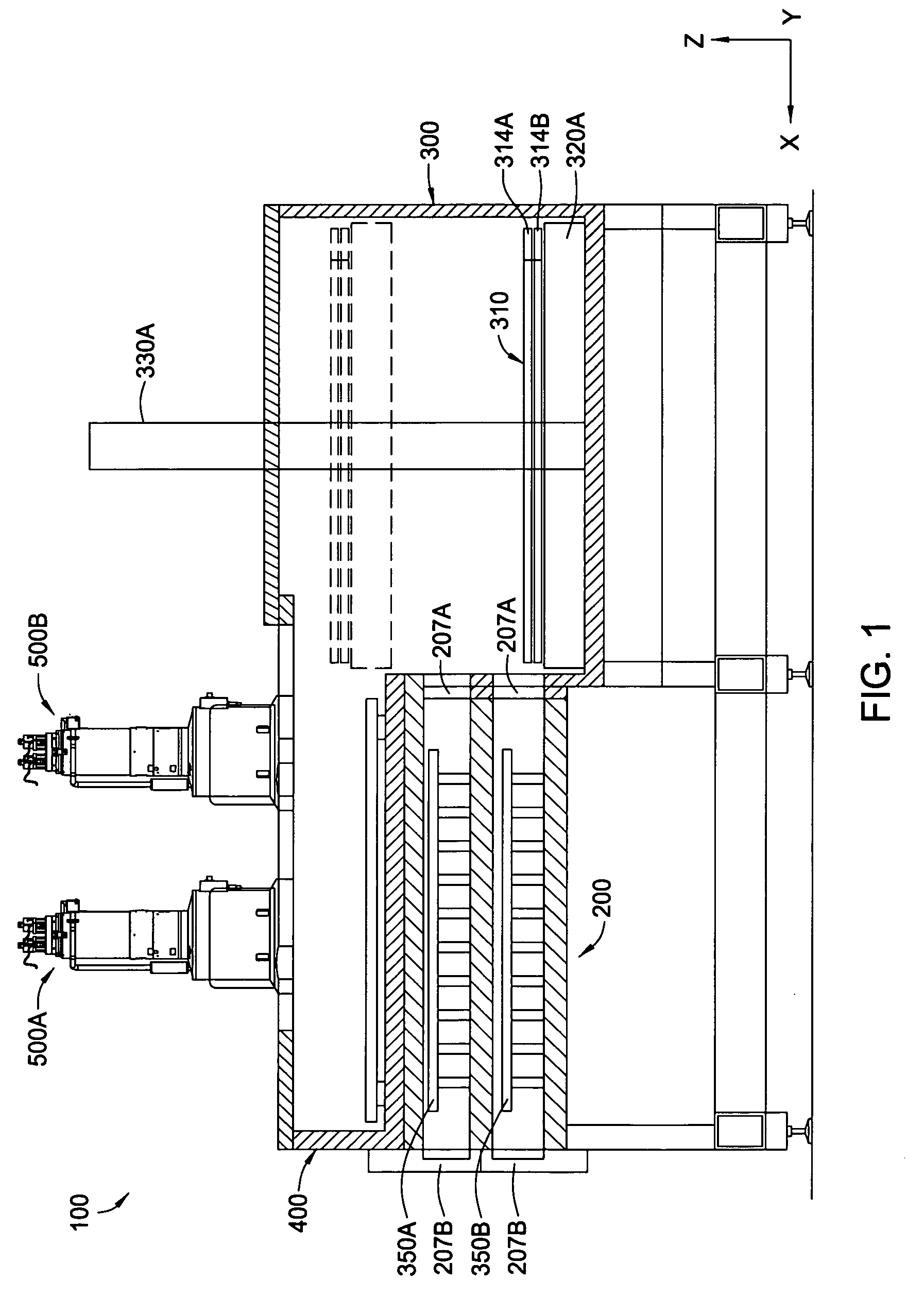
[0022] An electron test system and method for using the same are provided. The test system is an integrated system requiring minimum space, and is capable of testing substrates of from 15,000 mm2 or more. The term “substrate” as used herein refers to a flat panel display substrate, and includes a glass substrate having one or more thin film transistors disposed thereon.

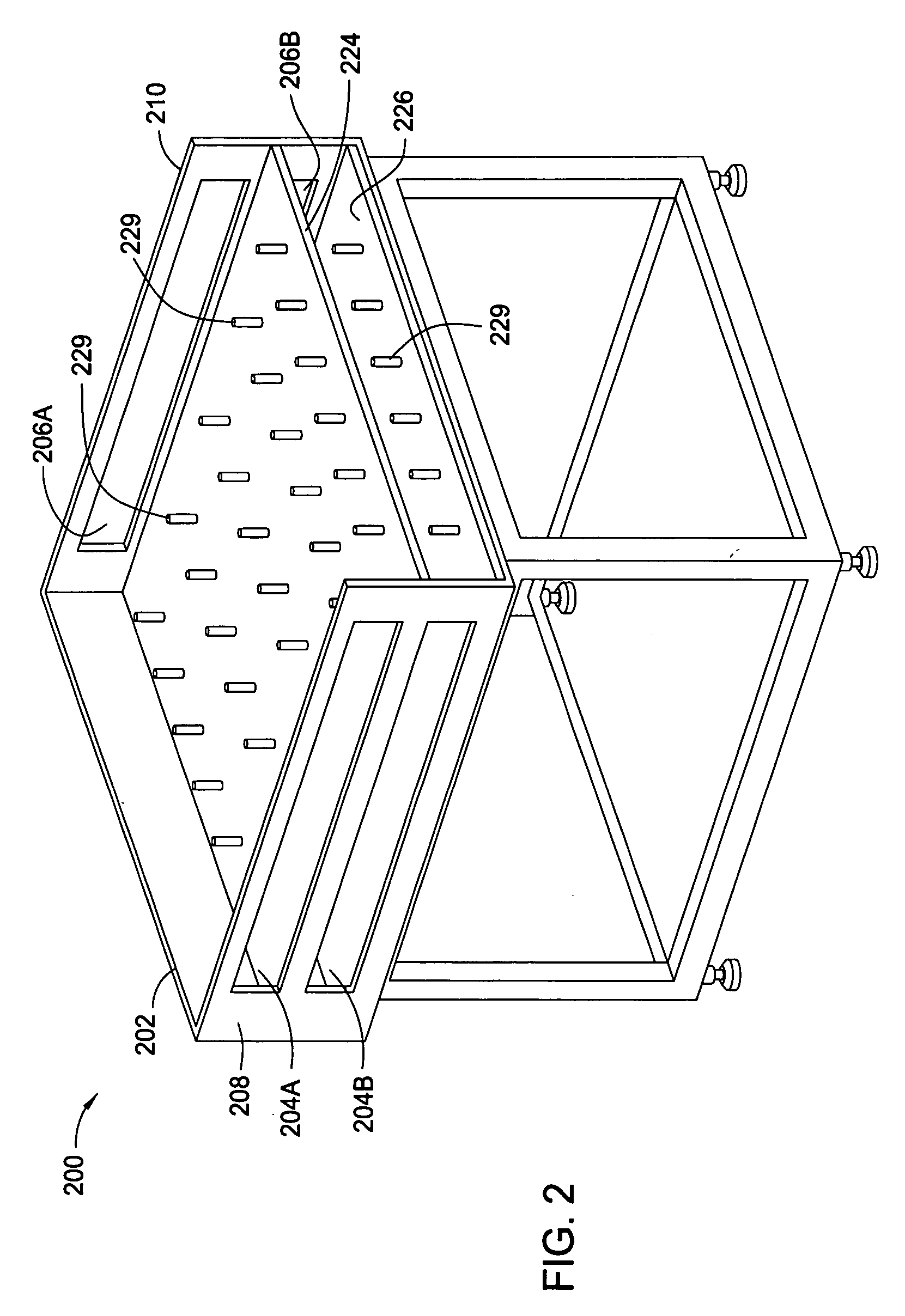
[0023] In one or more embodiments, the test system includes a load lock chamber, a transfer chamber, a testing chamber, and one or more test columns. In one or more embodiments, at least a portion of the load lock chamber is mounted below the testing chamber and adjacent the transfer chamber. In one or more embodiments, the testing chamber is integrated with a transfer chamber and disposed adjacent a load lock chamber. In any one or more of the embodiments identified above or elsewhere herein, the transfer chamber, the load lock chamber, and the testing chamber share a common environment which is typically maintained...


PUM


Abstract

A method and system for testing one or more large substrates are provided. In one or more embodiments, the system includes a testing chamber having a substrate table disposed therein. The substrate table is adapted to move a substrate within the testing chamber in various directions. More particularly, the substrate table includes a first stage movable in a first direction, and a second stage movable in a second direction, wherein each of the stages moves in an X-direction, Y-direction or both X and Y directions. The system further includes a load lock chamber at least partially disposed below the testing chamber, and a transfer chamber coupled to the load lock chamber and the testing chamber. In one or more embodiments, the transfer chamber includes a robot disposed therein which is adapted to transfer substrates between the load lock chamber and the testing chamber.

Description

BACKGROUND OF THE INVENTION [0001] 1. Field of the Invention [0002] Embodiments of the invention generally relate to an electronic test system for large substrates. More particularly, embodiments of the invention generally relate to an electron beam test system for large glass panel substrates. [0003] 2. Description of the Related Art [0004] Active matrix liquid crystal displays (LCDs) are commonly used for applications such as computer and television monitors, cell phone displays, personal digital assistants (PDAs), and an increasing number of other devices. Generally, an active matrix LCD includes two substrates, such as two glass panels for example with a layer of liquid crystal materials held therebetween. One of the substrates typically includes a conductive film formed thereon. The other substrate typically includes an array of thin film transistors (TFTs) coupled to an electrical power source. Each TFT may be switched on or off to generate an electrical field between a TFT an...

Claims


Application Information

Patent Timeline
Patent Type & Authority Applications(United States)
IPC IPC(8): G01R31/26
CPCG01R31/2886H01J2237/204H01J37/185
Inventor BRUNNER, MATTHIASKURITA, SHINICHIBLONIGAN, WENDELL T.KEHRBERG, EDGAR
Owner APPLIED MATERIALS INC
Why Eureka
Try Eureka