Multi-lens light emitting diode

a light-emitting diode and multi-lens technology, applied in the field of light-emitting diodes, can solve the problems of not being able to disclose any means for realizing a beam angle exceeding 160°, and neither disclose any solution

Active Publication Date: 2006-02-16
SAMSUNG ELECTRONICS CO LTD
View PDF3 Cites 157 Cited by
  • Summary
  • Abstract
  • Description
  • Claims
  • Application Information

AI Technical Summary

Problems solved by technology

However, this approach also fails to disclose any means for realizing a beam angle exceeding 160°.
In addition, this approach neither discloses any solution for realizing a narrow beam angle in a specific range.

Method used


Image

  • Multi-lens light emitting diode
  • Multi-lens light emitting diode
  • Multi-lens light emitting diode

Examples


first embodiment

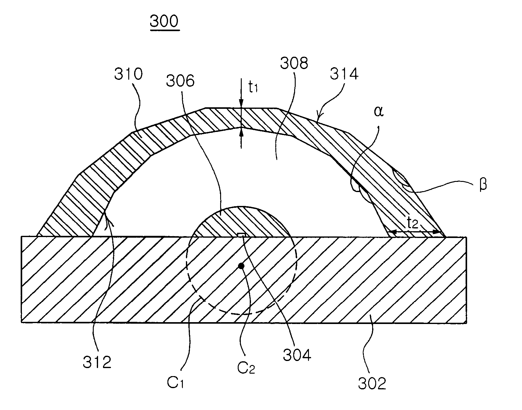
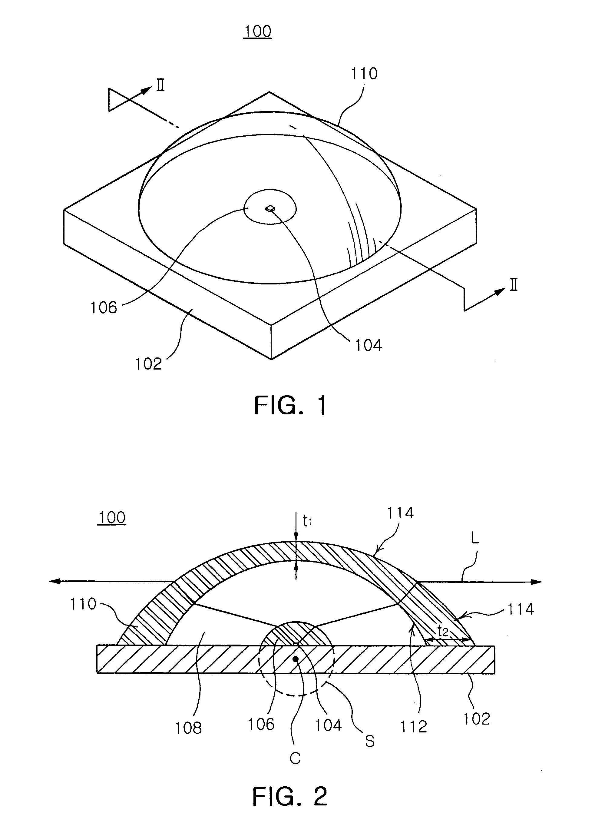
[0036] As shown in FIGS. 1 to 3, a multi-lens LED 100 according to the invention includes a board 102 printed with patterns (not shown), an LED chip 104 mounted on the board 102, a first lens 106 for sealing the LED chip 104 and a second lens 110 placed around the first lens 106 at a predetermined space. In addition, an intermediate air layer 108 is form of the air filled between the first and second lenses 106 and 110.

[0037] Though not shown in FIGS. 1 to 3, the multi-lens LED 100 of the invention also has several components provided in the board 102 like a typical LED. These components include leads for supplying external voltage to the LED chip 104, a semi-elliptical reflector for reflecting light emitted from the LED chip 104 in an upward direction and a metal pad for radiating heat generated from the LED chip 104 to the outside.

[0038] The first and second lenses 106 and 110 are molded from transparent resin, and alternatively, may be formed of other transparent material such a...

second embodiment

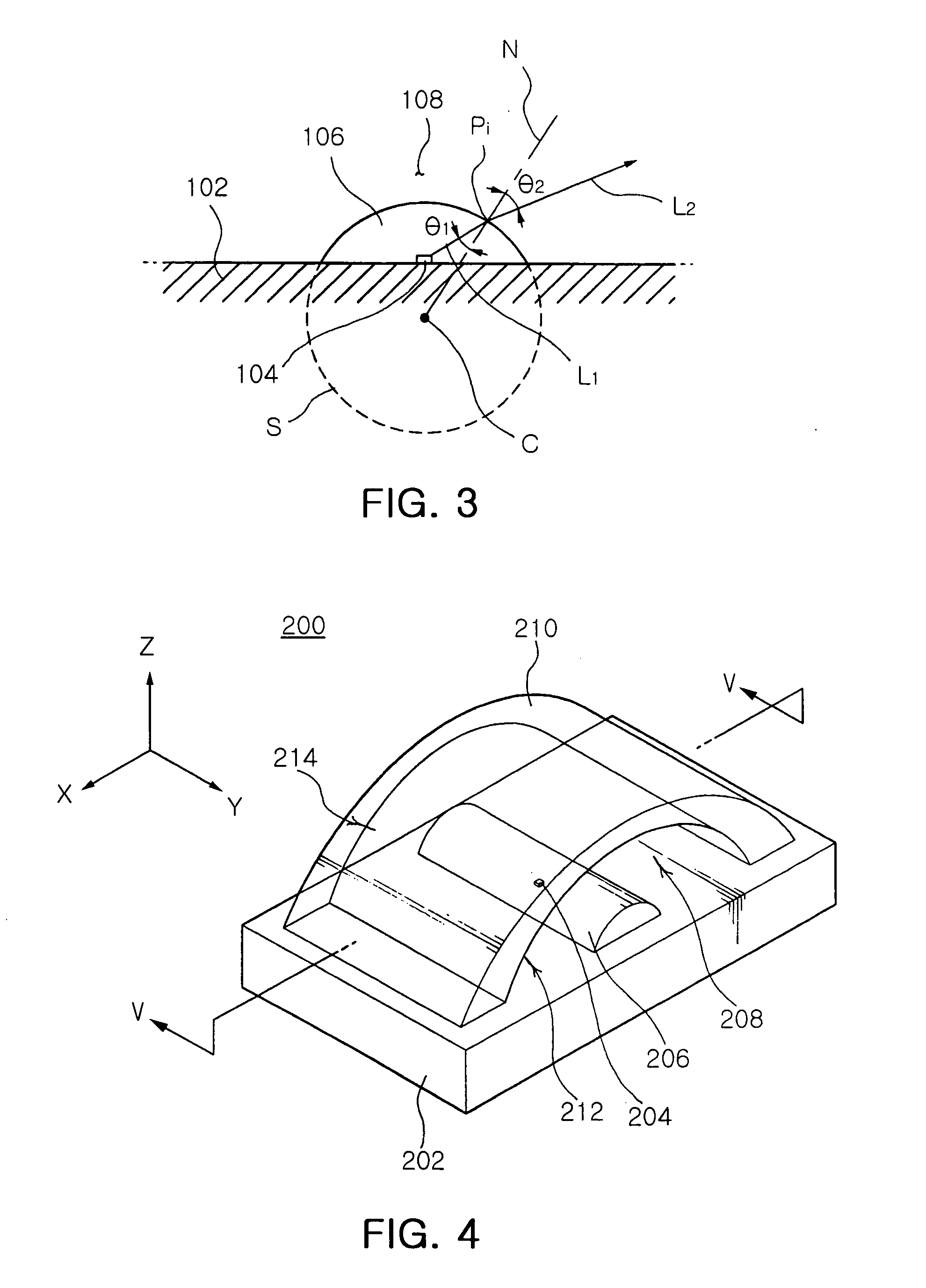
[0053] As shown in FIGS. 4 to 6, a multi-lens LED 200 according to the invention includes a board 202 printed with patterns (not shown), an LED chip 204 mounted on the board 202, a first lens 206 for sealing the LED chip 204 and a second lens 210 placed around the first lens 206 at a predetermined space. In this case, an intermediate layer 208 is formed of the air filled between the first and second lenses 206 and 210. The first and second lenses 206 and 210 are shaped as a partial cylinder that is taken along the y-axis.

[0054] Though not shown in FIGS. 4 to 6, the multi-lens LED 200 of the invention also has several components provided in the board 202 like a typical LED. These components include leads for supplying external voltage to the LED chip 204, a semi-elliptical reflector 216 for reflecting light emitted from the LED chip 204 in an upward direction and a metal pad for radiating heat generated from the LED chip 204 to the outside.

[0055] As shown in FIG. 6, the reflector 21...


PUM


Abstract

The present invention relates to a multi-lens LED. The LED has multiple lenses and an intermediate layer interposed between the multiple lenses in order to radiate light emitted from an LED chip in a desired direction and / or beam angle without using a complicated lens configuration. The first lens is centered behind the LED chip when seen in the propagation direction of light, the second lens has a concave structure and surrounds the first lens, and the intermediate layer is interposed between the first and second lenses, so that light emitted from the LED chip can be radiated in a wide beam angle. When provided in the form of a hemisphere, the multi-lens LED can be attached to a wall or a ceiling in use for interior lighting. On the other hand, when provided in the form of a cylinder, the multi-lens LED of the invention can be applied in arrays to be used as a light source of an LCD backlight apparatus.

Description

RELATED APPLICATION [0001] The present application is based on, and claims priority from, Korean Application Number 2004-63630, filed on Aug. 12, 2004, the disclosure of which is hereby incorporated by reference herein in its entirety. BACKGROUND OF THE INVENTION [0002] 1. Field of the Invention [0003] The present invention relates to a Light Emitting Diode (LED), more particularly, which has multiple lenses and an intermediate layer between the lenses in order to radiate light from an LED chip in a desired direction and / or beam angle without using a complicated lens configuration. [0004] 2. Description of the Related Art [0005] A typical LED is fabricated by a following process, in which an LED chip is placed on a reflector, the chip are connected with leads via wires, and resin material for example transparent resin is molded over a resultant structure. Then, light beams emitted from the LED chip are radiated to the outside in a specific beam angle according to the geometry of the...

Claims


Application Information

Patent Timeline
Patent Type & Authority Applications(United States)
IPC IPC(8): F21V13/04H01L33/54H01L33/58
CPCG02F1/133603Y10S362/80H01L33/58H01L33/54
Inventor PARK, JUNG KYUPARK, YOUNG SAMHAHM, HUN JOOJEONG, YOUNG JUNEKIM, HYUNG SUK
Owner SAMSUNG ELECTRONICS CO LTD
Why Eureka
Try Eureka