SELF HEATING MONITOR FOR SiGe AND SOI CMOS DEVICES

a self-heating monitor and soi cmos technology, applied in the direction of instruments, nuclear engineering, nuclear elements, etc., can solve the problems of increasing the device's susceptibility to thermal effects, poor thermal conductivity properties, and extremely limited thermal pathways on the island of sig

Active Publication Date: 2006-03-02
GLOBALFOUNDRIES US INC
View PDF12 Cites 13 Cited by
  • Summary
  • Abstract
  • Description
  • Claims
  • Application Information

AI Technical Summary

Problems solved by technology

Such large temperature effects in SGOI devices are due in part to the active region of the device being almost entirely surrounded by layers of material having poor thermal conductivity properties.
Due to the surrounding oxide, the SiGe island has extremely limited thermal pathways by which to dissipate any heat generated in the SiGe island.
The small dimensions of the SiGe island also increase the device's susceptibility to thermal effects.
As such, the SiGe island itself fails to act as its own heat sink for the device and the device quickly heats the island up to the devices own temperature.
However, such a method is difficult to implement because it is difficult to build such a diode close to a device to be measured to provide an accurate gauge of the active region of the device.
While simple to fabricate such a temperature measurement configuration, the data produced by such a configuration is less than reliable because of various hysteresis-like effects.
Such a sensitivity to electrical history makes determining the actual temperature of the device to be less than reliable.

Method used


Image

  • SELF HEATING MONITOR FOR SiGe AND SOI CMOS DEVICES
  • SELF HEATING MONITOR FOR SiGe AND SOI CMOS DEVICES
  • SELF HEATING MONITOR FOR SiGe AND SOI CMOS DEVICES

Examples


Embodiment Construction

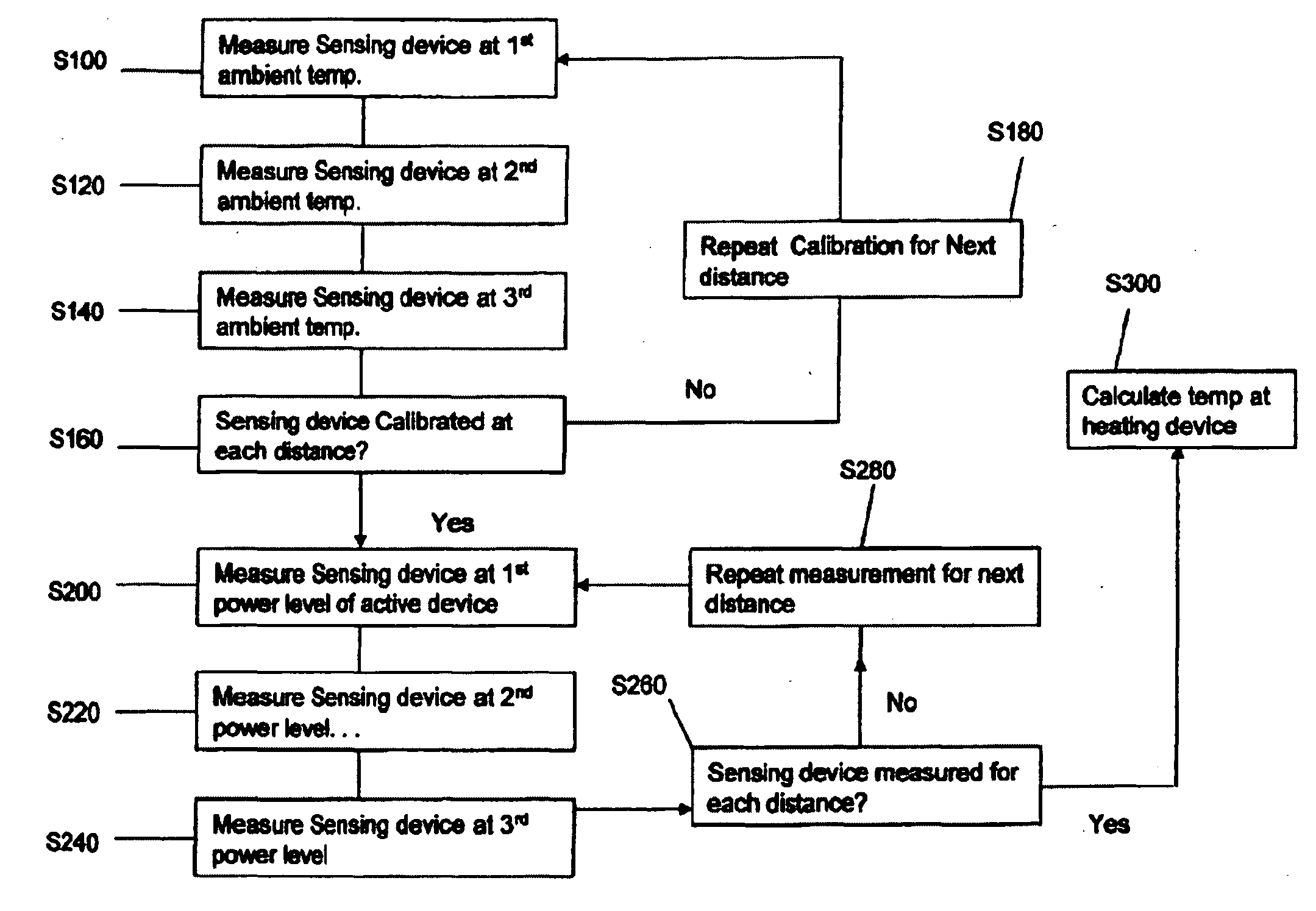
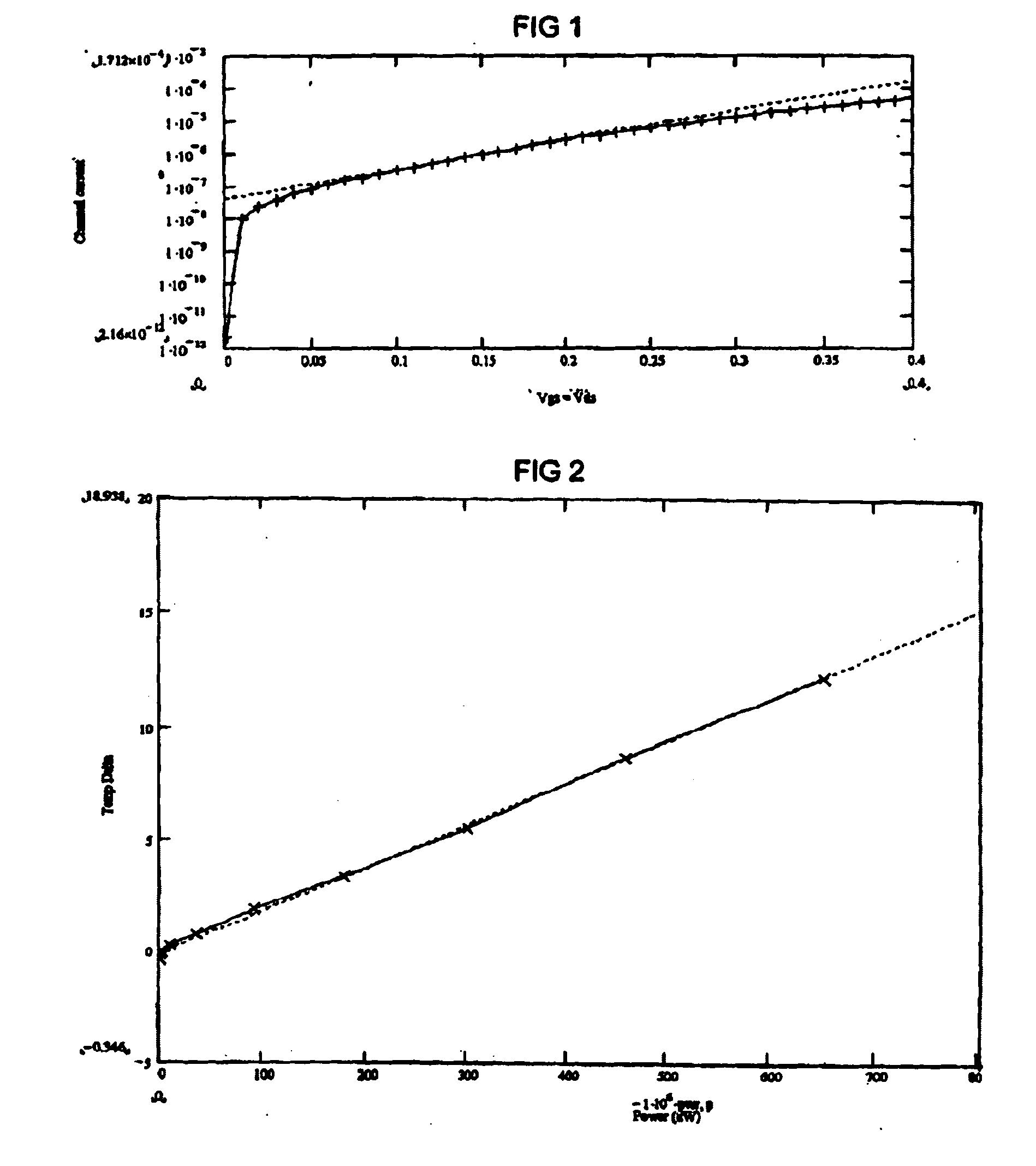
[0024] The invention is directed to determining the temperature of an active region of a device fabricated using SGOI technology as a function of electrical power through the device. Such information may be used to characterize the effect of temperature on the performance characteristics of the device. This information may be utilized by design engineers to predict device performance during the circuit layout process, as a function of temperature, and to accommodate such temperature effects in the circuit design.

[0025] To reliably measure the temperature of a semiconductor device, and thereby determine the effects on performance of the device, a method includes fabricating two devices in thermal communication with one another, where the first device is run at a predetermined power level, and the second device is a prescribed distance from the first device. The second device, otherwise known as the measuring device, is capable of providing temperature information at its position as ...


PUM


Abstract

A structure, apparatus and method for deterring the temperature of an active region in semiconductor, particularly a FET is provided. A pair FETs are arranged on a silicon island a prescribed distance from one another where the silicon island is surrounded by a thermal insulator. One FET is heated by a current driven therethrough. The other FET functions as a temperature sensor by having a change in an electrical characteristic versus temperature monitored. By arranging multiple pairs of FETs separated by different known distances, the temperature of the active region of one of the FETs may be determined during operation at various driving currents.

Description

BACKGROUND OF THE INVENTION [0001] 1. Field of the Invention [0002] The invention relates to semiconductor circuit design, and more particularly to modeling temperatures of a self-heating semiconductor device. [0003] 2. Background Description [0004] Accurate measurement of self-heating of SOI and SiGe based MOSFET devices is important because DC currents of such devices are typically depressed significantly due to self-heating. This is in contrast to CMOS circuits where transients are too rapid for significant self-heating to occur. Thus, simulation (compact) models must be adjusted to correctly account for self-heating in order to correctly predict circuit performance. In SOI technologies, this effect ranges from about 3 percent to 12 percent, while in SGOI (SiGe on SOI) these effects are expected to exceed 30 percent. [0005] Such large temperature effects in SGOI devices are due in part to the active region of the device being almost entirely surrounded by layers of material havin...

Claims


Application Information

Patent Timeline
Patent Type & Authority Applications(United States)
IPC IPC(8): G06F15/00G21C17/00G06F11/30
CPCG01N27/18
Inventor HYDE, PAUL A.NOWAK, EDWARD J.
Owner GLOBALFOUNDRIES US INC
Why Eureka
Try Eureka