
Semi-transmission type liquid crystal display which reflects incident light coming from outside to provide a display light source and transmits light from a light source at the back

a liquid crystal display and incident light technology, applied in static indicating devices, instruments, non-linear optics, etc., can solve the problems of reducing the efficiency of rubbing process, and reducing the intensity of rubbing process, so as to reduce the effect of color chang

Inactive Publication Date: 2006-03-30
NEC LCD TECH CORP
View PDF13 Cites 2 Cited by
  • Summary
  • Abstract
  • Description
  • Claims
  • Application Information

AI Technical Summary

Benefits of technology

This design optimizes the intensity of output light in both reflection and transmission modes, prevents the need for multiple thin film transistors, and reduces production costs by simplifying drive voltage control, while ensuring effective alignment and improved display characteristics.

Problems solved by technology

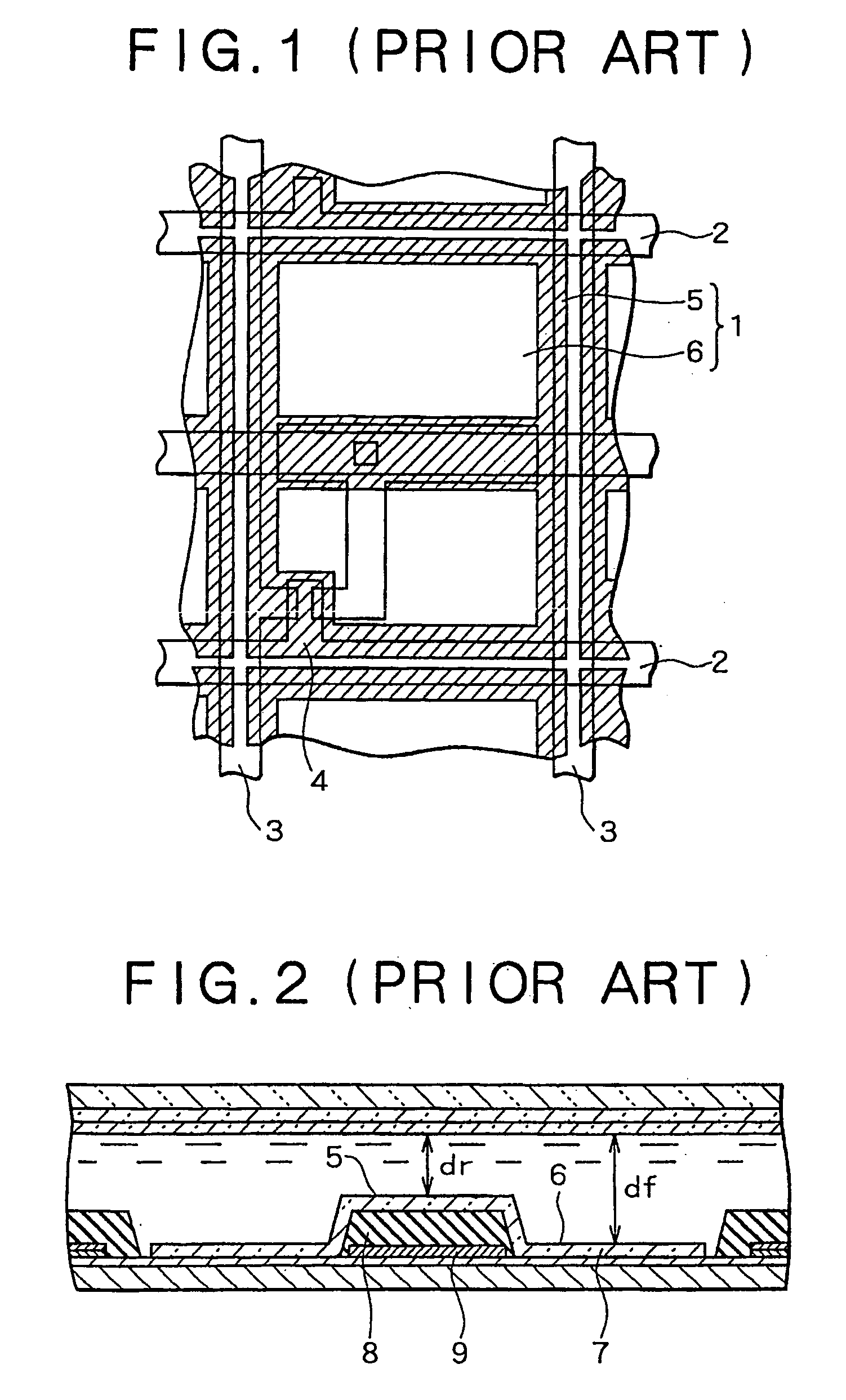
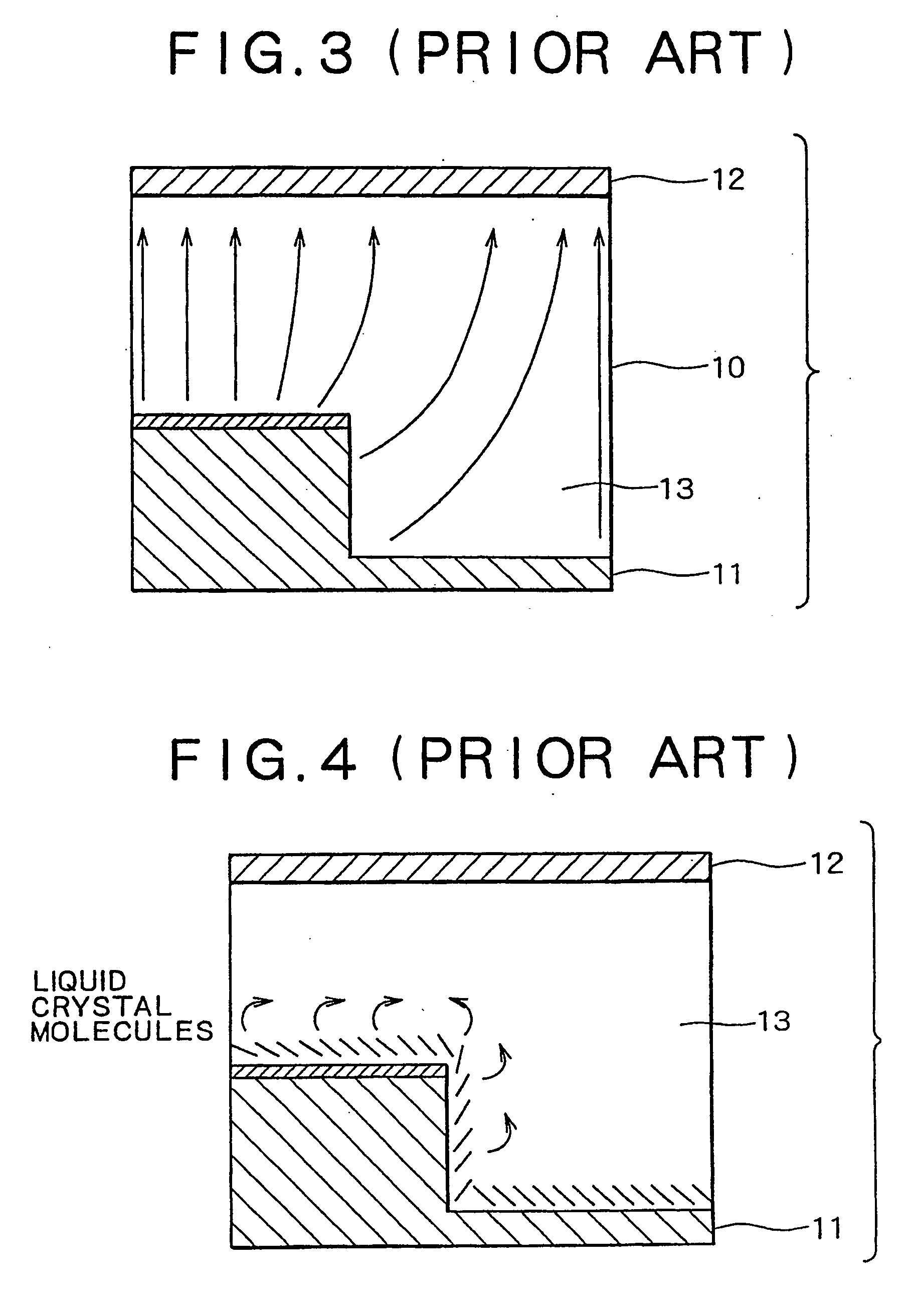
This results in a retardation difference between both areas, which disables the maximization of the intensity of the output light.
This brings about a problem of making effective alignment difficult in a rubbing process.

Method used


Image

  • Semi-transmission type liquid crystal display which reflects incident light coming from outside to provide a display light source and transmits light from a light source at the back
  • Semi-transmission type liquid crystal display which reflects incident light coming from outside to provide a display light source and transmits light from a light source at the back
  • Semi-transmission type liquid crystal display which reflects incident light coming from outside to provide a display light source and transmits light from a light source at the back

Examples


first embodiment

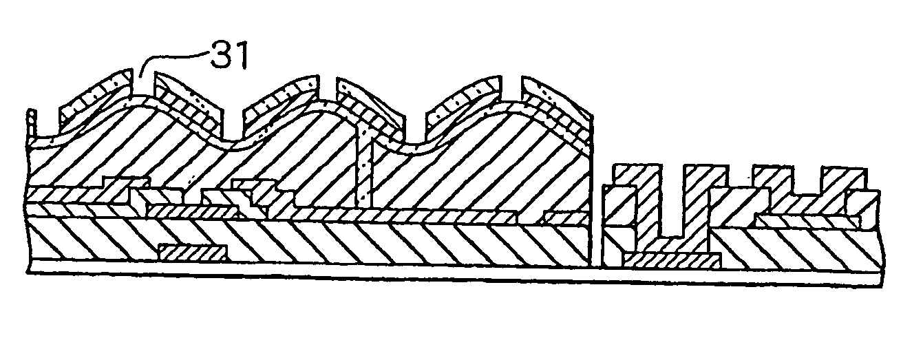
[0062]FIG. 6 is a partial cross-sectional view of a semi-transmission type liquid crystal display according to the invention. As shown in FIG. 6, the semi-transmission type liquid crystal display has, inside, a lower substrate 11, an opposite substrate 12 so arranged as to face the lower substrate 11 and a liquid crystal layer 13 sandwiched between the lower substrate 11 and the opposite substrate 12. The semi-transmission type liquid crystal display employs an active matrix system which has, for example, thin film transistors (TFTs) provided as switching elements pixel by pixel.

[0063] The lower substrate 11 has an insulative substrate 14, an insulating protection film 15, TFTs 16, an insulating layer 17, a reflection electrode 18 and a transparent electrode 19. The insulating protection film 15 is deposited on the insulative substrate 14 and the TFTs 16 are formed on the insulating protection film 15. Each TFT 16 has a gate electrode 16a on the insulative substrate 14, a drain elec...

second embodiment

[0076]FIG. 10 is a cross-sectional view showing a part of the lower substrate of the second embodiment in a simplified form. A contact hole 20 reaching the source electrode 16d of the TFT 16 is bored in the insulating layer 17. The reflection electrode 18 and transparent electrode 19 are deposited, covering the contact hole 20 and the insulating layer 17. The transparent electrode 19 is connected to the source electrode 16d of the TFT 16 and has a function to serve as a pixel electrode. The reflection electrode 18 is electrically connected to the transparent electrode 19 via an insulating film 21 and has a function to serve as a reflector and a pixel electrode. The transparent insulating film 21 of SiO2 or the like is deposited on the reflection electrode 18. At this time, the insulating film 21 is deposited on the entire surface of the reflection electrode 18 in such a way as to completely cover the reflection electrode 18. Although not illustrated, an alignment film 22 of polyimid...

fourth embodiment

[0093]FIG. 14 is a cross-sectional view showing a part of the lower substrate of the fourth embodiment in a simplified form. A contact hole 20 reaching the source electrode 16d of the TFT 16 is bored in the insulating layer 17. The transparent electrode 19, the insulating film 21 and the reflection electrode 18 are deposited, covering the contact hole 20 and the insulating layer 17. The transparent electrode 19 is connected to the source electrode 16d of the TFT 16 and has a function to serve as a pixel electrode. The transparent insulating film 21 of SiO2 or the like is deposited between the transparent electrode 19 and the reflection electrode 18. The reflection electrode 18 is electrically connected to the transparent electrode 19 via an insulating film 21 and has a function to serve as a reflector and a pixel electrode.

[0094] The insulating layer 17 has an undulating surface and the transparent electrode 19 and the reflection electrode 18 deposited on the insulating layer 17 als...


PUM

PropertyMeasurementUnit
reflection areaaaaaaaaaaa
transparentaaaaaaaaaa
voltageaaaaaaaaaa

Abstract

A semi-transmission type liquid crystal display that maximizes the luminance in reflection mode and transmission mode. The liquid crystal display comprises a lower substrate with thin film transistors, an opposite substrate facing the lower substrate, a liquid crystal layer between the lower substrate and the opposite substrate, a reflection electrode formed in a reflection area of the lower substrate, a transparent electrode formed in a transparent area of the lower substrate, a common electrode formed on the opposite substrate, and a drive circuit for applying a voltage between the reflection electrode and the transparent electrode and the common electrode. The potential difference between a drive voltage applied to that surface of the lower substrate which contacts the liquid crystal layer and a drive voltage applied to that surface of the opposite substrate which contacts the liquid crystal layer is lower in the transparent area than in the reflection area.

Description

CROSS REFERENCE TO RELATED APPLICATION [0001] This application is a divisional of U.S. patent application Ser. No. 11 / 009,506, filed Dec. 10, 2004, which is, in turn, a continuation of U.S. patent application Ser. No. 10 / 216,967, filed Aug. 12, 2002, now U.S. Pat. No. 6,831,715, issued Dec. 14, 2004.BACKGROUND OF THE INVENTION [0002] 1. Field of the Invention [0003] The present invention relates to a liquid crystal display, and, more particularly, to a semi-transmission type liquid crystal display which reflects incident light coming from outside to provide a display light source and transmits light from a light source at the back. [0004] 2. Description of the Related Art [0005] There is a reflection type liquid crystal display (LCD) known which has a reflector inside and reflects incident external light by the reflector to provide a display light source, thereby eliminating the need for a backlight as a light source and a transmission type liquid crystal display equipped with a bac...

Claims


Application Information

Patent Timeline
Patent Type & Authority Applications(United States)
IPC IPC(8): G02F1/1335G02F1/133G02F1/1343
CPCG02F1/136227G02F1/133555G02F1/1343
Inventor IKENO, HIDENORISUZUKI, MASAYOSHI
Owner NEC LCD TECH CORP
Learn More