

Multi-chip stack package
a stack package and stack technology, applied in the direction of semiconductor devices, semiconductor/solid-state device details, electrical apparatus, etc., can solve problems such as short circuits, and achieve the effects of avoiding short circuits of bonding wires, reducing the connection length of bonding wires, and avoiding long bonding wires
- Summary
- Abstract
- Description
- Claims
- Application Information
AI Technical Summary
Benefits of technology
Problems solved by technology
Method used
Image

Examples
first embodiment
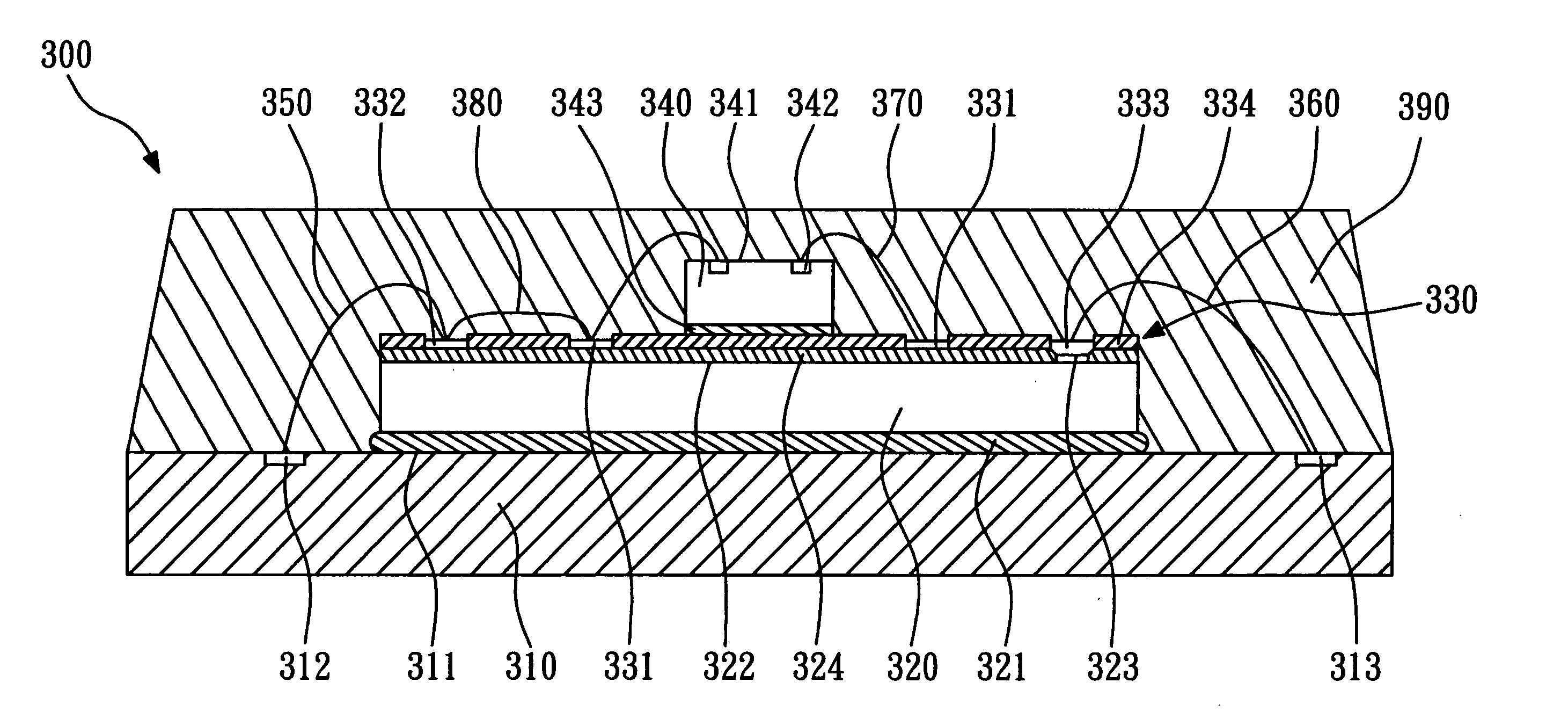
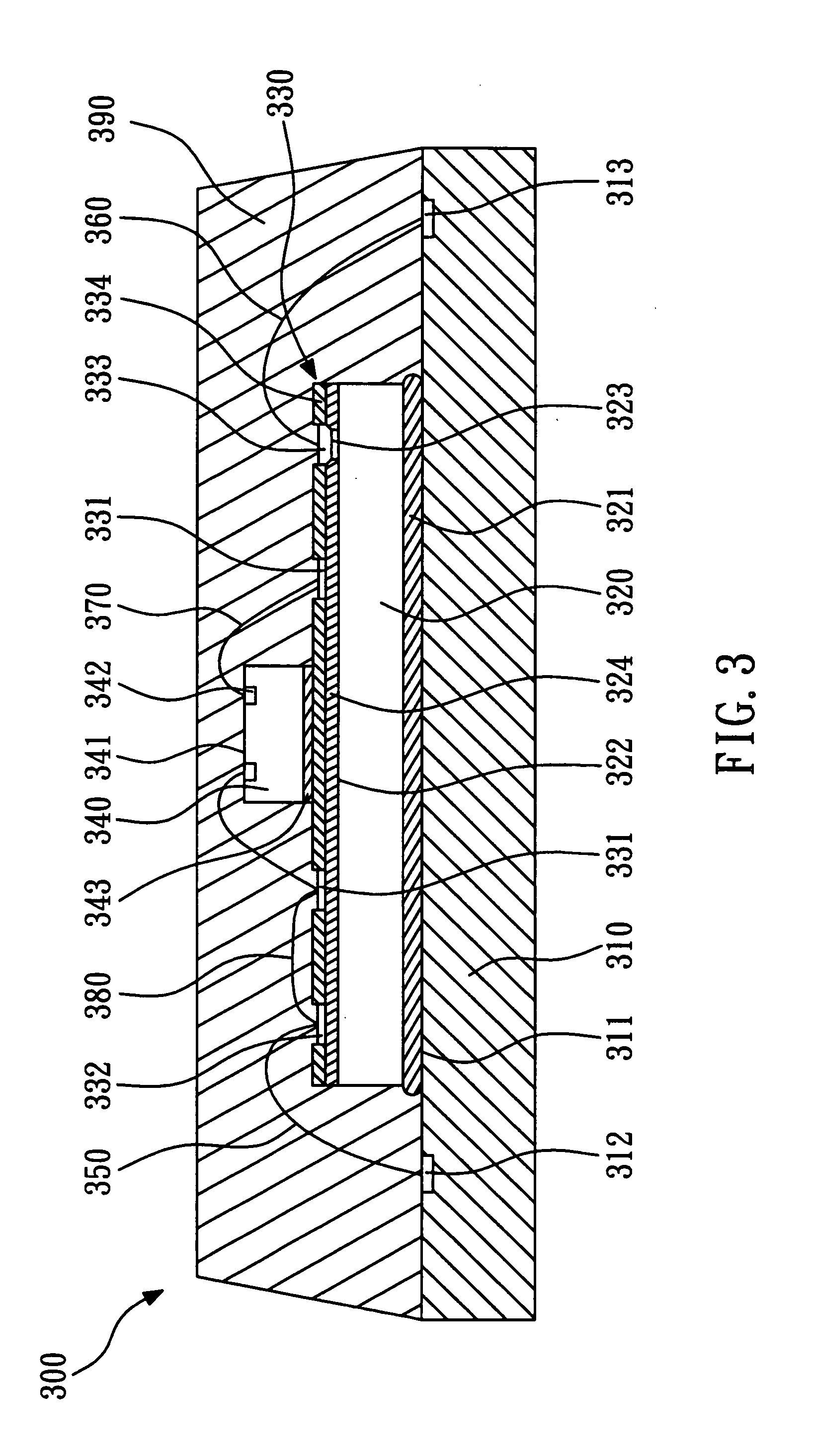
[0015] Referring to FIG. 3, according to the present invention, a multi-chip stack package 300 mainly comprises a substrate 310, a first chip 320, a redistribution structure 330, a second chip 340, and a plurality of first bonding wires 350. The substrate 310 comprises an upper surface 311 and a plurality of connecting pads 312, 313 formed on the upper surface 311. The substrate 310 can be a printed circuit board. The first chip 320 comprises a first active surface 322 and a plurality of bonding pads 323 formed on the first active surface 322, and it is stacked on the upper surface 311 of the substrate 310 through an adhesive 321, by the first active surface 322 facing upwards. In this embodiment, the first bonding pads 323 are arranged at the periphery of the first active surface 322. A passivation layer 324 is formed on the first active surface 322, and exposes the first bonding pads 323. The first chip 320 can be a memory chip.
[0016] The redistribution structure 330 comprises a p...
second embodiment
[0020] Referring to FIG. 4, according to the present invention, a multi-chip stack package 400 mainly comprises a substrate 410, a first chip 420, a redistribution structure 430, a second chip 440, a third chip 450, and a plurality of first bonding wires 460. The substrate 410 comprises an upper surface 411 and a plurality of connecting pads 412, 413 formed on the upper surface 411.
[0021] The first chip 420 comprises a first active surface 422 and a plurality of first bonding pads 423 formed on the first active surface 422. The first chip 420 is attached to the upper surface 411 of the substrate 410 through an adhesive 421, by the first active surface 422 facing upwards. A passivation layer 424 is formed on the first active surface 422 and exposes the first bonding pads 423.
[0022] The redistribution structure 430 formed on the first active surface 422 of the first chip 420 comprises a plurality of first intermediate pads 431, a plurality of second intermediate pads 432, a plurality...
PUM
 Abstract
Description
Claims
Application Information