SRAM cells having landing pad in contact with upper and lower cell gate patterns and methods of forming the same

a technology of sram cells and gate patterns, applied in the field of sram cells having a landing pad in contact with upper and lower cell gate patterns, can solve the problems of weak latch-up immunity and lower integration density of sram cells in bulk cmos

Active Publication Date: 2006-05-11
SAMSUNG ELECTRONICS CO LTD
View PDF3 Cites 4 Cited by
  • Summary
  • Abstract
  • Description
  • Claims
  • Application Information

AI Technical Summary

Problems solved by technology

However, the bulk CMOS SRAM cell may have lower integration density as well as weaker latch-up immunity as compared to the TFT SRAM cell.

Method used


Image

  • SRAM cells having landing pad in contact with upper and lower cell gate patterns and methods of forming the same
  • SRAM cells having landing pad in contact with upper and lower cell gate patterns and methods of forming the same
  • SRAM cells having landing pad in contact with upper and lower cell gate patterns and methods of forming the same

Examples


Embodiment Construction

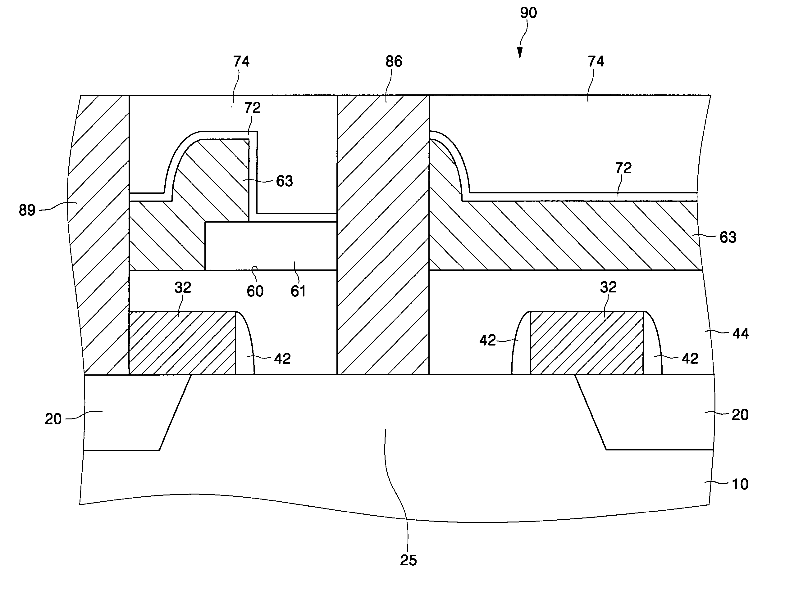
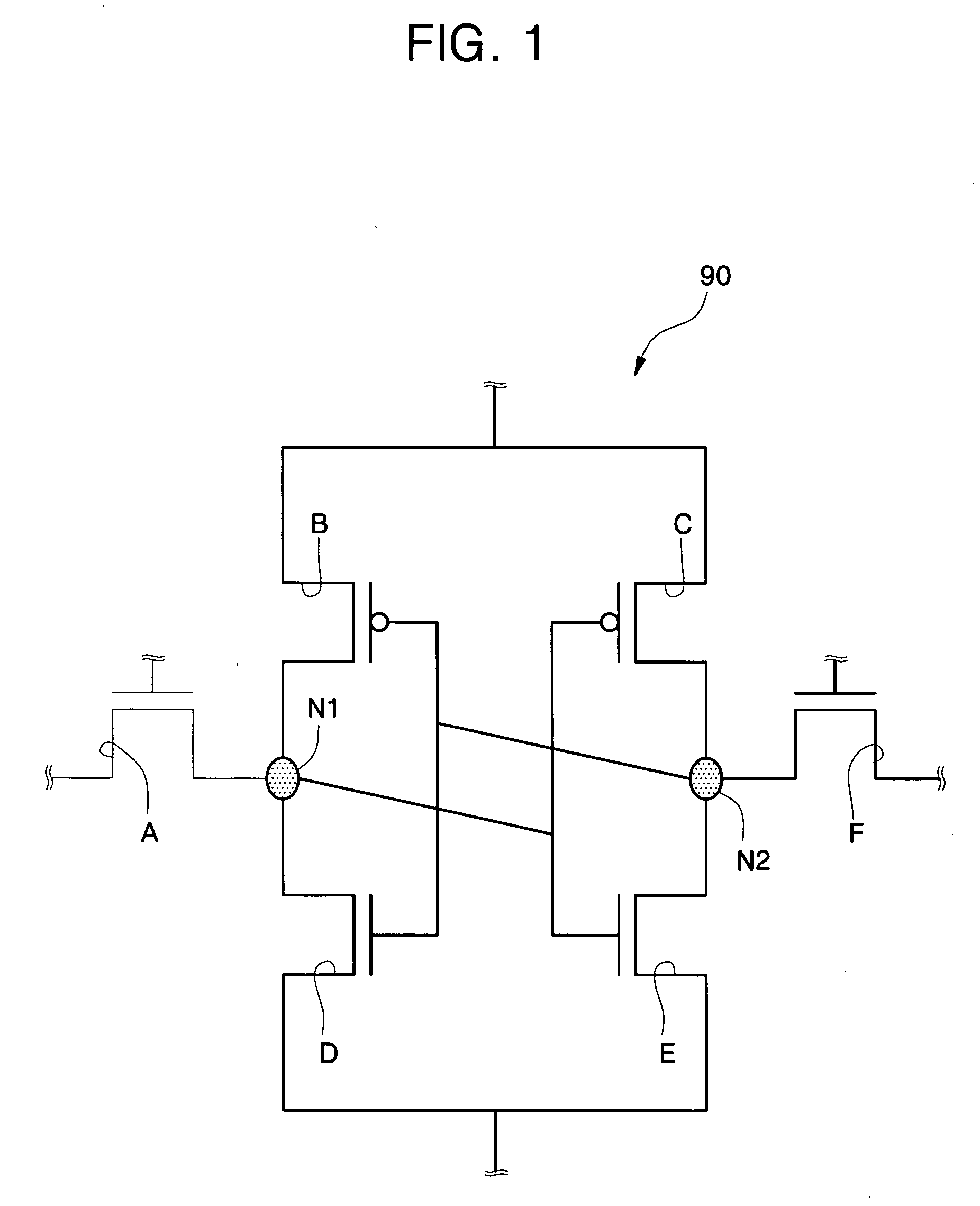
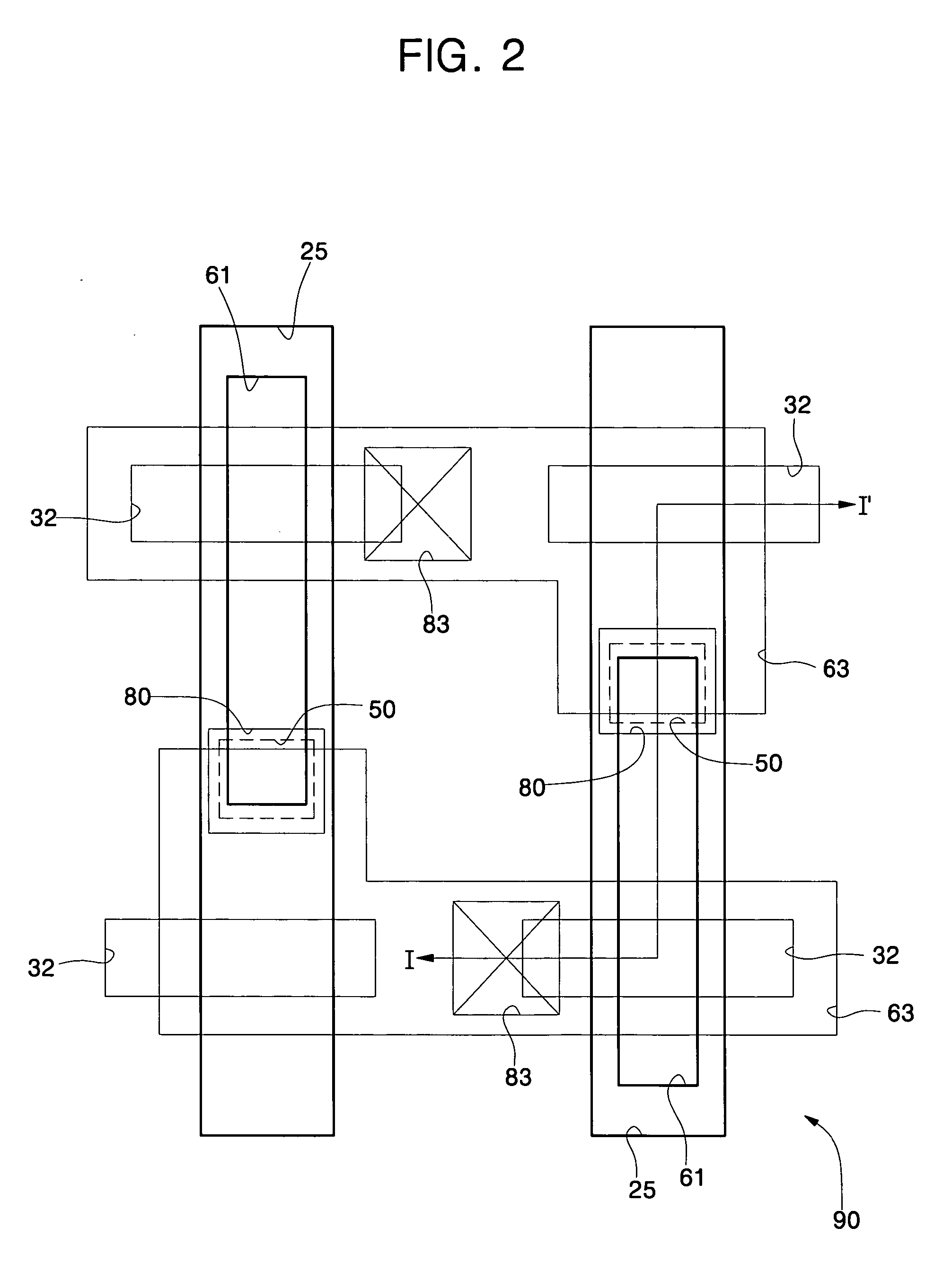
[0020]FIG. 1 is a circuit diagram illustrating an SRAM cell in a cell array region according to the present invention, and FIG. 2 is a layout view illustrating the SRAM cell of FIG. 1. Further, FIG. 3 is a cross sectional view of the SRAM cell taken along line I-I′ of FIG. 2.

[0021] Referring to FIGS. 1 to 3, an SRAM cell normally has six transistors A, B, C, D, E, and F within one cell of a cell array region. The transistors A, B, C, D, E, and F constitute a latch structure and show electrical characteristics of the latch structure. That is, two transistors B and D among the transistors A, B, C, D, E, and F are connected to one electrical node N2 together with three opposite transistors C, E, and F. And two transistors C and E among the transistors A, B, C, D, E, and F are connected to the other electrical node N1 together with three opposite transistors A, B, and D. At this time, two transistors B and C among the transistors A, B, C, D, E, and F are P-type MOSFET (Metal Oxide Semi...


PUM


Abstract

SRAM cells having landing pads in contact with upper and lower cell gate patterns, and methods of forming the same are provided. The SRAM cells and the methods remove the influence resulting from structural characteristics of the SRAM cells having vertically stacked upper and lower gate patterns, for stably connecting the patterns on the overall surface of the semiconductor substrate. An isolation layer isolating at least one lower active region is formed in a semiconductor substrate of the cell array region. The lower active region has two lower cell gate patterns. A body pattern is disposed in parallel with the semiconductor substrate. The body pattern is formed to confine an upper active region, which has upper cell gate patterns on the lower cell gate patterns. A landing pad is disposed between the lower cell gate patterns. A node pattern is formed to simultaneously contact the upper cell gate pattern and the lower cell gate pattern.

Description

CROSS-REFERENCE TO RELATED APPLICATION [0001] This patent application claims priority from Korean Patent Application No. 10-2004-0090608, filed Nov. 8, 2004, the contents of which are hereby incorporated by reference in their entirety. BACKGROUND OF INVENTION [0002] 1. Technical Field [0003] The present invention relates to SRAM (Static Random Access Memory) cells and methods of forming the same, and more particularly, to SRAM cells having a landing pad in contact with upper and lower cell gate patterns and methods of forming the same. [0004] 2. Discussion of the Related Art [0005] In semiconductor memory devices, a static random access memory (SRAM) device may offer advantages of lower power consumption and faster operating speed as compared to a dynamic random access memory (DRAM) device. Therefore, the SRAM may be widely used for cache memory in computer and / or other portable devices. [0006] A unit cell of a SRAM device mat be categorized as either a resistor-load SRAM cell or a ...

Claims


Application Information

Patent Timeline
Patent Type & Authority Applications(United States)
IPC IPC(8): H01L29/76
CPCG11C11/412H01L27/11H01L27/1108Y10S257/903H10B10/00H10B10/125H10B99/00
Inventor KIM, SUNG-JINJUNG, SOON-MOONCHO, WON-SEOKJANG, JAE-HOONKWAK, KUN-HOKIM, JONG-HYUKSHIM, JAE-JOO
Owner SAMSUNG ELECTRONICS CO LTD
Why Eureka
Try Eureka