Method for fabricating 3d-nonvolatile memory device

a memory device and non-volatile technology, applied in the direction of semiconductor devices, basic electric elements, electrical equipment, etc., can solve the problems of difficulty in realizing further increase in integration using lithography technology

Inactive Publication Date: 2012-09-13
SK HYNIX INC
View PDF2 Cites 89 Cited by
  • Summary
  • Abstract
  • Description
  • Claims
  • Application Information

AI Technical Summary

Benefits of technology

[0009]In accordance with another embodiment of the present invention, a method for fabricating a 3D-nonvolatile memory device includes: forming a sub-channel over a substrate; forming a stacked layer over the substrate, the stacked layer including a plurality of interlayer dielectric layers that are alternatively stacked with conductive layers; selectively etching the stacked layer to form a first open region exp...

Problems solved by technology

For example, there are difficulties in realizing fur...

Method used


Image

  • Method for fabricating 3d-nonvolatile memory device
  • Method for fabricating 3d-nonvolatile memory device
  • Method for fabricating 3d-nonvolatile memory device

Examples


first embodiment

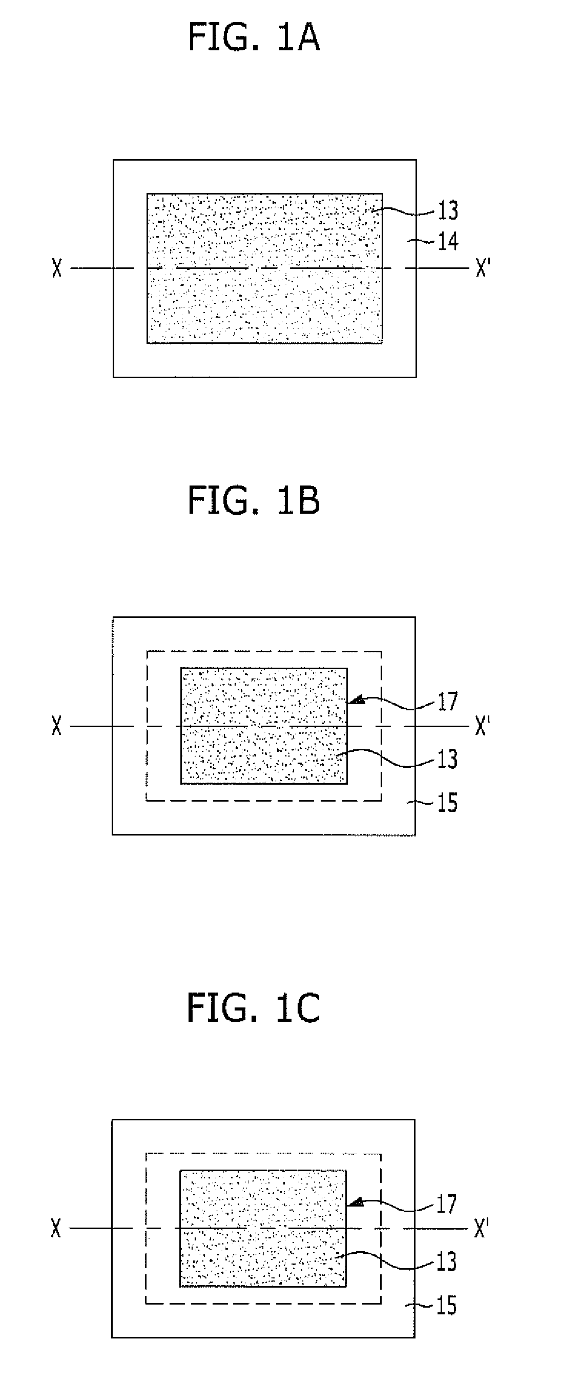
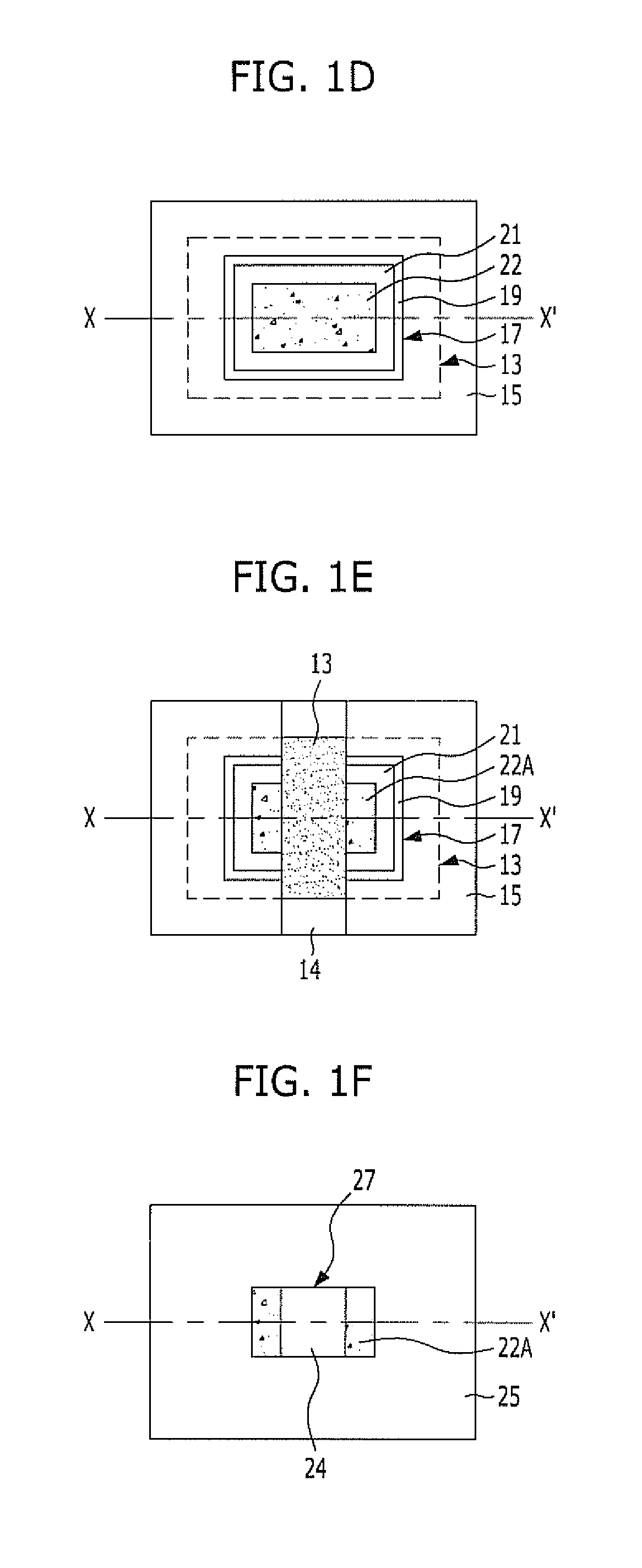
[0016]FIGS. 1A to 1G are plan views illustrating a method for fabricating a 3D-nonvolatile memory device in accordance with the present invention. FIGS. 2A to 2G are cross-sectional views taken along lines X-X′ of FIGS. 1A to 1G, respectively.

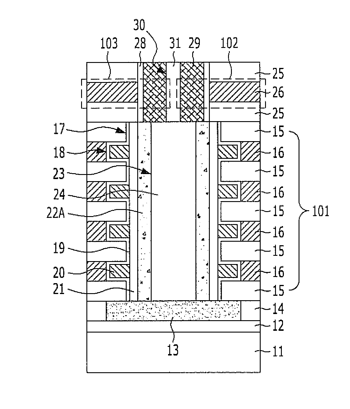
[0017]Referring to FIGS. 1A and 2A, a buried insulation layer 12 is formed on a substrate 11 (shown in FIG. 2A). The buried insulation layer 12 in FIG. 2A serves to electrically isolate the substrate 11 from a sub-channel 13 which is to be formed by a subsequent process. The buried insulation layer 12 may be formed of oxide.

[0018]An insulation layer 14 is formed on the buried insulation layer 12 to electrically isolate the sub-channel 13 from an adjacent sub-channel 13. The sub-channel 13 serves to electrically couple a plurality of main channels which are to be formed by a subsequent process. The sub-channel 13 may be formed of any one selected from the group consisting of a silicon layer, a metallic layer, and a nano tube. The metallic layer ...

second embodiment

[0038]FIGS. 3A to 3d are plan views illustrating a method for fabricating a 3D-nonvolatile memory device in accordance with the present invention. FIGS. 4A to 4D are cross-sectional views taken along X-X′ lines of FIGS. 3A to 3D, respectively.

[0039]Referring to FIGS. 3A and 4A, an insulation layer 44 is formed on a substrate 41 having a buried insulation layer 42 formed thereon. The insulation layer 44 serves to electrically isolate a sub-channel 43 from an adjacent sub-channel 43.

[0040]A stacked layer 201 is formed on the substrate 41 having the sub-channel 43 formed thereon. The stacked layer 210 includes a plurality of interlayer dielectric layers 45 and conductive layers 46 which are alternately stacked. The numbers of the interlayer dielectric layers 45 and the conductive layers 46 to be stacked may be adjusted according to the number of memory cells (MC) to be implemented.

[0041]The stacked layer 201 is selectively etched to form a first open region 47 exposing the sub-channel ...


PUM


Abstract

A method for fabricating a 3D-nonvolatile memory device includes forming a sub-channel over a substrate, forming a stacked layer over the substrate, the stacked layer including a plurality of interlayer dielectric layers that are alternatively stacked with conductive layers, selectively etching the stacked layer to form a first open region exposing the sub-channel, forming a main-channel conductive layer to gap-fill the first open region, selectively etching the stacked layer and the main-channel conductive layer to form a second open region defining a plurality of main channels, and forming an isolation layer to gap-fill the second open region.

Description

CROSS-REFERENCE TO RELATED APPLICATIONS[0001]The present application claims priority of Korean Patent Application No. 10-2011-0019859, filed on Mar. 7, 2011, which is incorporated herein by reference in its entirety.BACKGROUND[0002]1. Field[0003]Exemplary embodiments of the present invention relate to a method for fabricating a semiconductor device, and more particularly, to a method for fabricating a 3D-nonvolatile memory device.[0004]2. Description of the Related Art[0005]A nonvolatile memory device refers to a memory device which retains stored data, even though power supply is cut off. Currently, a variety of nonvolatile memory devices including a flash memory are being widely used.[0006]As further developments in the miniaturization and high integration of semiconductor devices are sought, device scaling is reaching limits while more memory cells are to be formed within a limited area to increase the memory capacity thereof. For example, there are difficulties in realizing furt...

Claims


Application Information

Patent Timeline
IPC IPC(8): H01L21/336
CPCH01L27/1203H01L27/11556H10B41/27H01L27/0688H10B41/35
Inventor JOO, HAN-SOOOH, SANG-HYUNPARK, YU-JIN
Owner SK HYNIX INC
Why Eureka
Try Eureka