Planar optical waveguide

a technology of optical waveguides and polymers, applied in the field of optical waveguides, can solve the problems of not teaching or suggesting the formation of optical waveguides, and none of the above prior art teaches or suggests the fabrication of master waveguides, and achieves the effect of convenient and inexpensive generation

Inactive Publication Date: 2006-05-11
PRINTPACK ILLINOIS
View PDF1 Cites 24 Cited by
  • Summary
  • Abstract
  • Description
  • Claims
  • Application Information

AI Technical Summary

Benefits of technology

[0011] In accordance with the present invention, a planar waveguide master having the physical form of optical elements formed therein is produced and polymer replicas are easily and inexpensively generated therefrom. This allows optical waveguides having optical components formed therein to be mass-produced.

Problems solved by technology

None of the above prior art teaches or suggests forming an optical waveguide from at least two polymer layers which have different indices of refraction.
Furthermore, none of the prior teaches or suggests fabricating a master waveguide having shaped optical elements formed therein and producing polymer optical waveguides from the master.

Method used


Image

  • Planar optical waveguide
  • Planar optical waveguide
  • Planar optical waveguide

Examples


Embodiment Construction

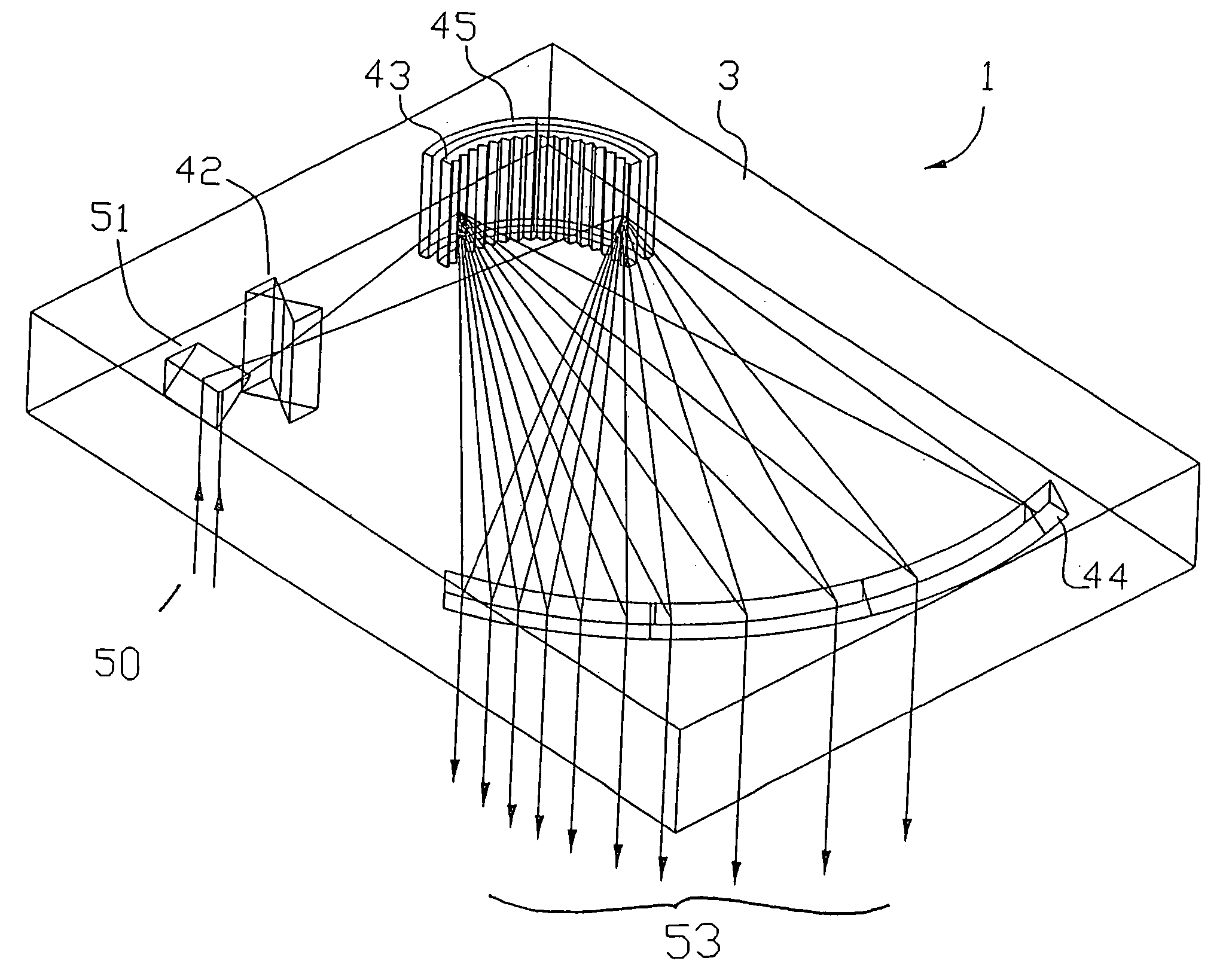
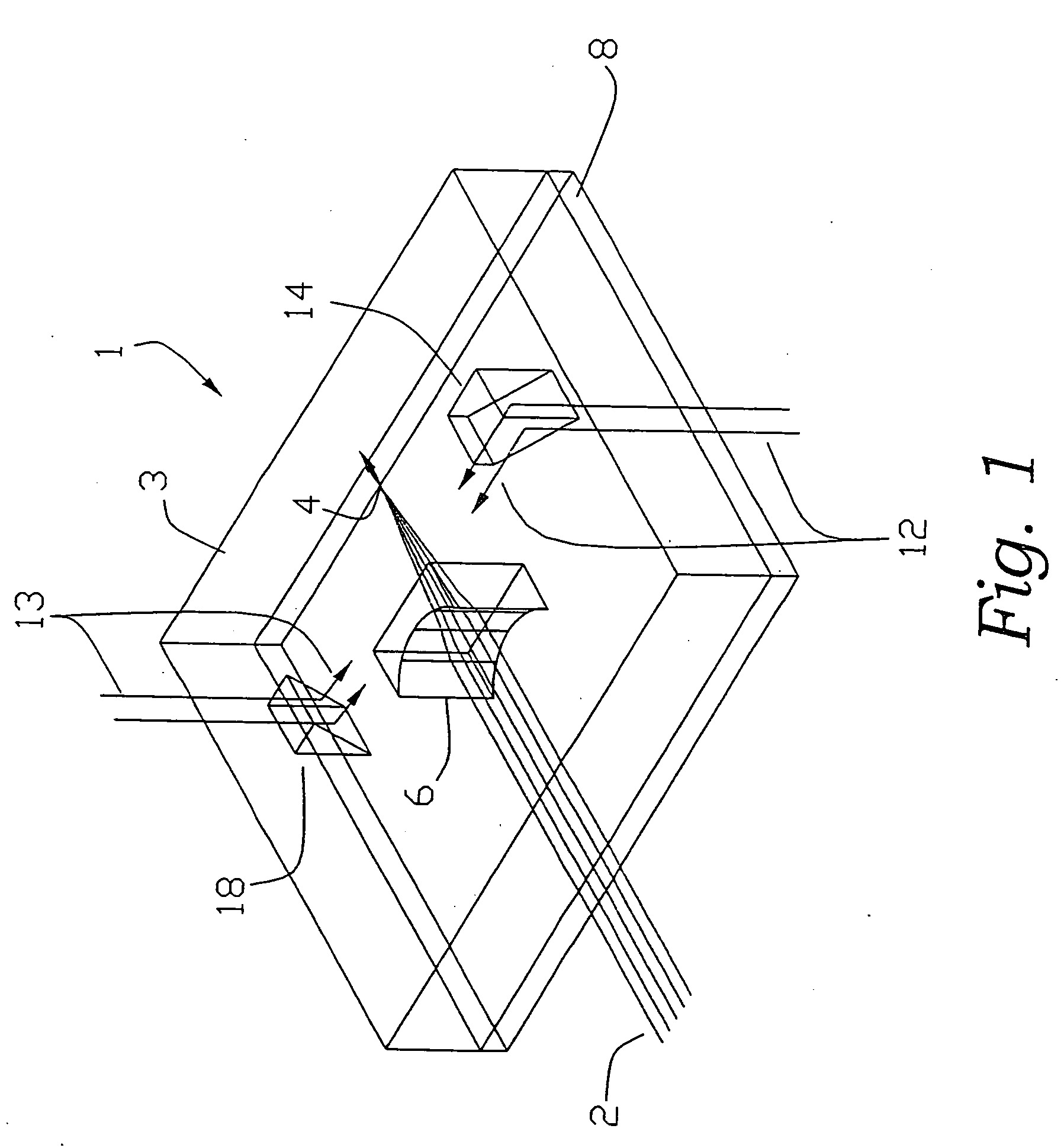
[0048]FIG. 1 illustrates the optical waveguide 1 of the present invention. Optical elements 6, 14 and 18 represent examples of the types of optical elements that can be formed in the optical waveguide 1. Light 2, 12, 13 projected into the light control device is manipulated by the optical elements in a predetermined manner. The optical elements are designed to receive light from a particular direction and to control the light in accordance with their optical properties. Therefore, the optical waveguide 1 can be created such that light projected into the optical waveguide from any predetermined direction will be received by an optical element and controlled in accordance with the optical characteristics of the particular optical element. The optical element that receives the light projected into the device will manipulate the light and transmit the light to other optical elements that further manipulate the light in accordance with their optical characteristics.

[0049] The optical wa...


PUM


Abstract

An embossed optical waveguide for light transmission and a method for creating a master and for generating the embossed optical waveguide therefrom. In accordance with an exemplary embodiment of the present invention, a layer of liquid polymer is exposed to energy curing radiation through a mask consisting of clear and opaque areas. The opaque areas in the mask correspond to areas in the liquid polymer which will not be exposed to the curing radiation. During exposure, the areas in the liquid polymer which are exposed through the clear areas in the mask to the curing radiation become cured, or hardened. The areas which are not exposed to the curing radiation do not become cured and subsequently are washed away with a chemical rinse. The resulting structure is a cured layer of polymer having holes pierced through it. The holes pierced through the polymer layer correspond to optical elements formed in the polymer layer. Alternatively, these optical elements can be formed in the layer of polymer after it is cured by reactive ion etching or ion beam milling. The polymer layer which has an index of refraction of 1.55 or greater is bonded to a substrate, which is preferably polypropylene, having an index of refraction of preferably 1.50 or less. Since the refractive index of air is approximately 1.0, the polymer layer is sandwiched between two layers of low refractive index material. The differences between the indices of refraction cause light projected into the polymer layer to be guided in the polymer layer by total internal reflection. Furthermore, once the optical elements have been formed in the polymer layer, it can be used as a master for generating embossments. The embossments are preferably generated by placing liquid polymer in contact with the master, curing it, and separating the cured polymer embossment from the master.

Description

RELATED APPLICATION [0001] This application claims priority from and the benefit of U.S. Provisional Patent Application Ser. No. 60 / 381,325 filed May 17, 2002.FIELD OF THE INVENTION [0002] The present invention relates to an optical waveguide having optical elements formed therein and, more particularly, to a polymer optical waveguide for light transmission having optical elements formed therein for optical computing, optical processing, and light control providing defined optical pathways, and a method for creating a master optical waveguide and for producing the polymer optical waveguide therefrom. BACKGROUND OF THE INVENTION [0003] It is generally known in the art that an optical waveguide can be created by placing layers of materials in contact with each other which have different indices of refraction such that light focused in the layer of material having the higher index of refraction will remain in that layer due to total internal reflection of the light at the boundaries be...

Claims


Application Information

Patent Timeline
Patent Type & Authority Applications(United States)
IPC IPC(8): G02B6/10G02B6/12G02B6/122G02B6/138
CPCB29D11/00663B42D25/29B82Y20/00G01J3/021G01J3/0259G02B6/12007G02B6/1221G02B6/1225G02B6/138G02B2006/12102G02B2006/12104G02B2006/12107G02B2006/12114G02B2006/1215G02B2006/12164B42D2035/20G02B6/10
Inventor STEENBLIK, RICHARD A.HURT, MARK J.
Owner PRINTPACK ILLINOIS
Why Eureka
Try Eureka