Memory cell with buffered layer

a memory cell and buffer layer technology, applied in the field of thin film resistance memory devices, can solve the problems of bipolar or unipolar, memory devices, and inability to change the cmr resistance, and achieve the effect of reliable programming

Active Publication Date: 2006-05-11
XENOGENIC DEV LLC
View PDF2 Cites 19 Cited by
  • Summary
  • Abstract
  • Description
  • Claims
  • Application Information

AI Technical Summary

Benefits of technology

[0010] The present invention provides a CMR memory device structure that can be reliably programmed using a bipolar pulse programming process. Alternately, the device can be programmed using a uni-polar pulse programming process. The flexibility in programming is a result of the device's unique buffered-layer design.

Problems solved by technology

However, when a high electric field induces current flow through the CMR material, a change in the CMR resistance can result.
A memory device that is responsive to only one type of programming, either bipolar or uni-polar, has a necessarily limited usefulness, and is dependent upon system specifications and available power supplies.
This uncertainty in the design of the memory cells necessarily increases production costs.
However, the CMR film composition can be a difficult variable to control.

Method used


Image

  • Memory cell with buffered layer
  • Memory cell with buffered layer
  • Memory cell with buffered layer

Examples


Embodiment Construction

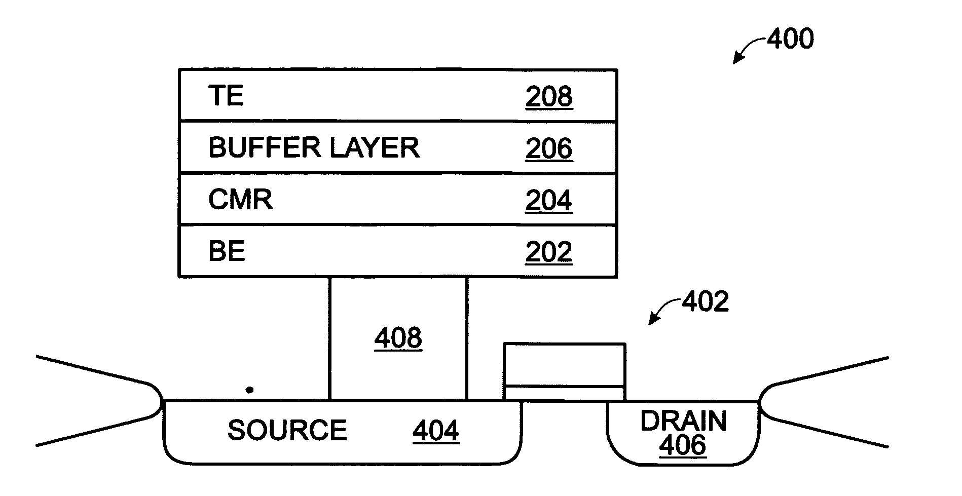
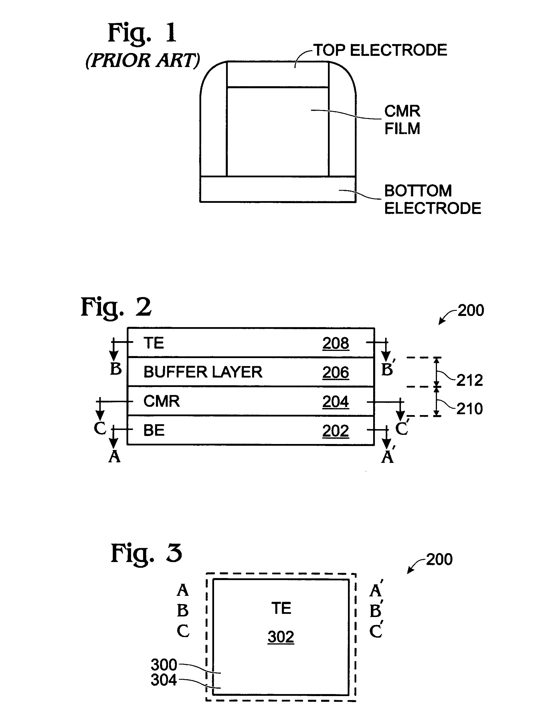
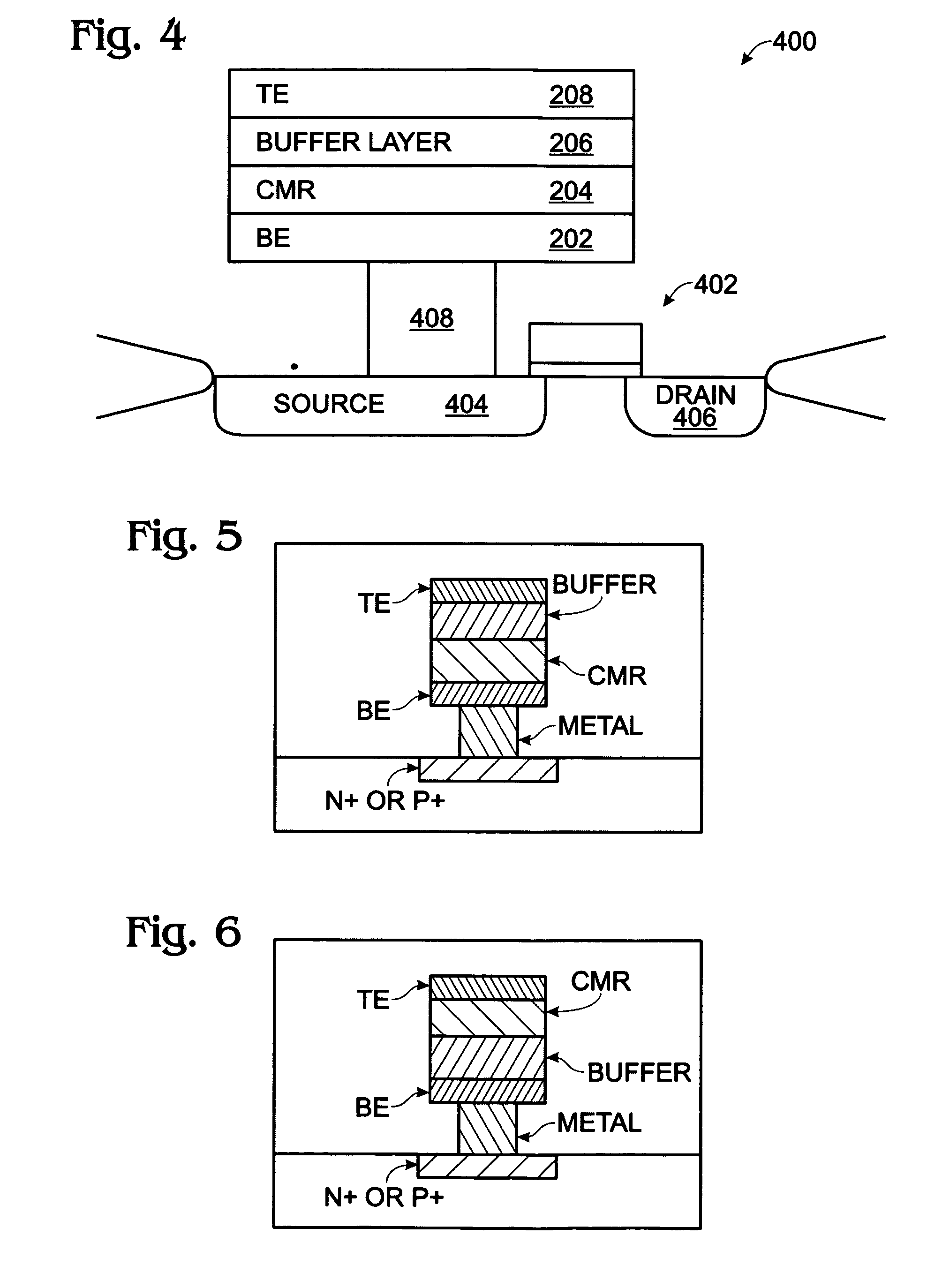
[0023]FIG. 2 is a partial cross-sectional view of the present invention buffered-layer memory cell. The memory cell 200 comprises a bottom electrode (BE) 202 and a CMR memory film 204 overlying the bottom electrode 202. A memory-stable semiconductor buffer layer 206 overlies the CMR memory film 204 and a top electrode (TE) 208 overlies the semiconductor buffer layer 206. Although the buffer layer 206 is shown adjacent the top electrode 208, in other aspects (see FIG. 6), the buffered layer 206 is adjacent the bottom electrode 202 and the CMR memory film 204 is adjacent the top electrode 208.

[0024]FIG. 3 is a plan view of the memory device 200 of FIG. 2. Considering both FIGS. 2 and 3, the top electrode 208 and bottom electrode 202 need not be asymmetric for the memory device 200 to be bipolar programmable. The programming aspects of the invention are discussed in more detail below. Alternately stated, the bottom electrode 202 has an area 300 (marked in phantom with dotted lines), w...


PUM


Abstract

A method is provided for forming a buffered-layer memory cell. The method comprises: forming a bottom electrode; forming a colossal magnetoresistance (CMR) memory film overlying the bottom electrode; forming a memory-stable semiconductor buffer layer, typically a metal oxide, overlying the memory film; and, forming a top electrode overlying the semiconductor buffer layer. In some aspects of the method the semiconductor buffer layer is formed from YBa2Cu3O7-X (YBCO), indium oxide (In2O3), or ruthenium oxide (RuO2), having a thickness in the range of 10 to 200 nanometers (nm). The top and bottom electrodes may be TiN / Ti, Pt / TiN / Ti, In / TiN / Ti, PtRhOx compounds, or PtIrOx compounds. The CMR memory film may be a Pr1-XCaXMnO3 (PCMO) memory film, where x is in the region between 0.1 and 0.6, with a thickness in the range of 10 to 200 nm.

Description

RELATED APPLICATIONS [0001] This application is a Continuation of a pending patent application entitled, BUFFERED-LAYER MEMORY CELL, invented by Hsu et al., Ser. No. 10 / 755,654, filed Jan. 12, 2004, which is a continuation-in-part of an issued patent entitled, ASYMMETRIC-AREA MEMORY CELL, invented by Hsu et al., U.S. Pat. No. 6,949,435, issued Sep. 27, 2005. Both of the above-mentioned applications are incorporated herein by reference.BACKGROUND OF THE INVENTION [0002] 1. Field of the Invention [0003] This invention generally relates to a thin film resistance memory device, for non-volatile memory arrays, and more particularly, to a bipolar programmable memory cell having a buffer layer adjacent an electrode. [0004] 2. Description of the Related Art [0005] State of the art resistor random access memories (RRAMs) are often made from a colossal magnetoresistance (CMR) memory film and, more typically, from a Pr0.7Ca0.3MnO3 (PCMO) type of CMR material. The CMR material can be said to ha...

Claims


Application Information

Patent Timeline
Patent Type & Authority Applications(United States)
IPC IPC(8): H01L21/00H01L21/20G11C13/00H01L27/10H01L27/24H01L45/00
CPCG11C13/0007G11C13/0069G11C2013/0073G11C2213/31G11C2213/51G11C2213/56G11C2213/79H01L27/101H01L45/12H01L45/04H01L45/1233H01L45/147H01L27/2436H10B63/30H10N70/801H10N70/20H10N70/826H10N70/8836
Inventor HSU, SHENG TENGLI, TINGKAIZHANG, FENGYANPAN, WEIZHUANG, WEI-WEIEVANS, DAVID R.TAJIRI, MASAYUKI
Owner XENOGENIC DEV LLC
Why Eureka
Try Eureka