High-dynamic range image sensors

a high-dynamic range, image sensor technology, applied in the direction of instruments, television systems, television system scanning details, etc., can solve the problem of limited dynamic range of existing cmos image sensors, and achieve the effect of extending the pixel range, reducing the cost of operation, and increasing the capacitan

Inactive Publication Date: 2006-06-22
PETING MARK
View PDF4 Cites 30 Cited by
  • Summary
  • Abstract
  • Description
  • Claims
  • Application Information

AI Technical Summary

Problems solved by technology

As set forth in the background, the dynamic range of existing CMOS image sensors is limited.

Method used


Image

  • High-dynamic range image sensors
  • High-dynamic range image sensors
  • High-dynamic range image sensors

Examples


Embodiment Construction

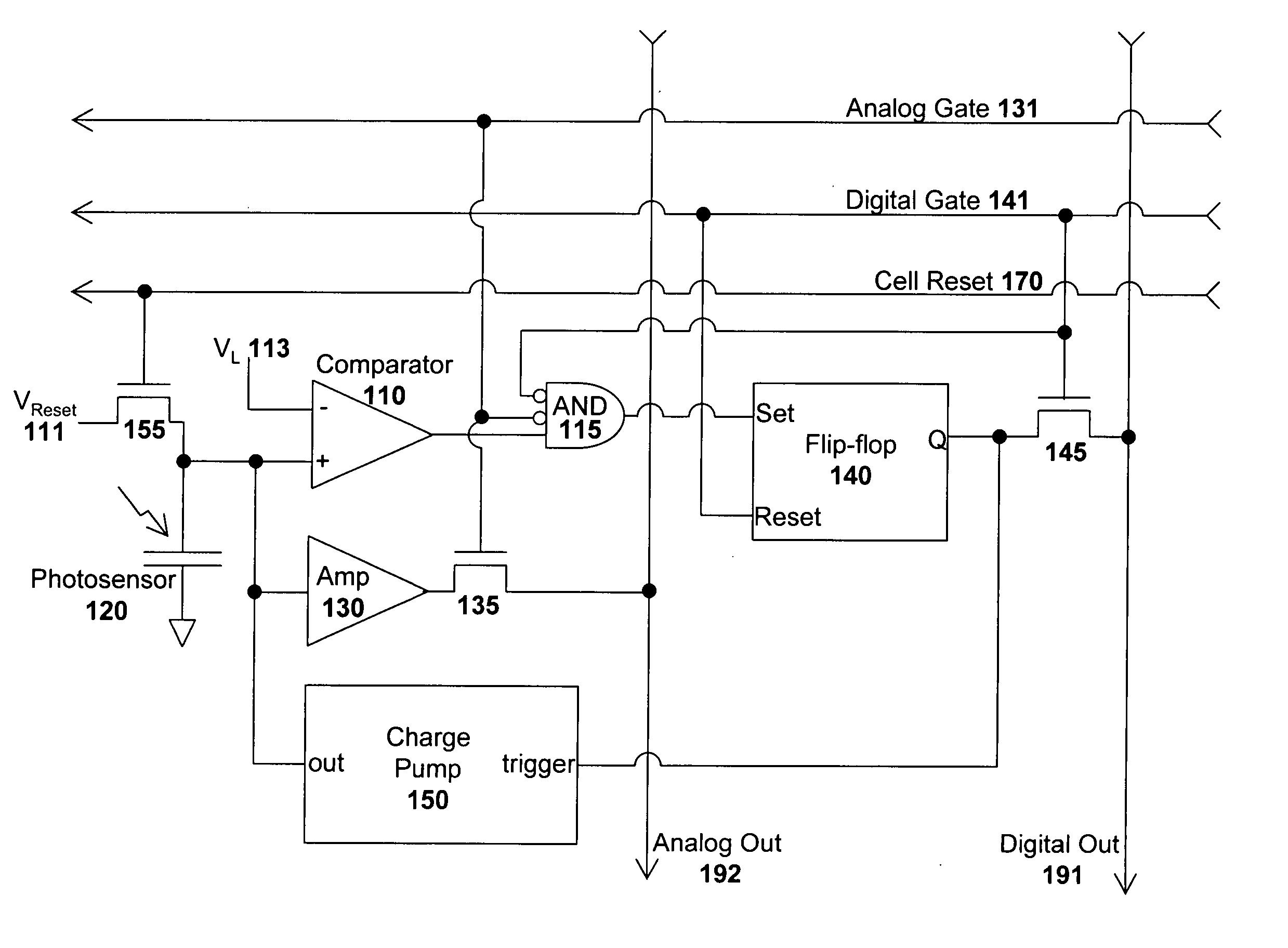
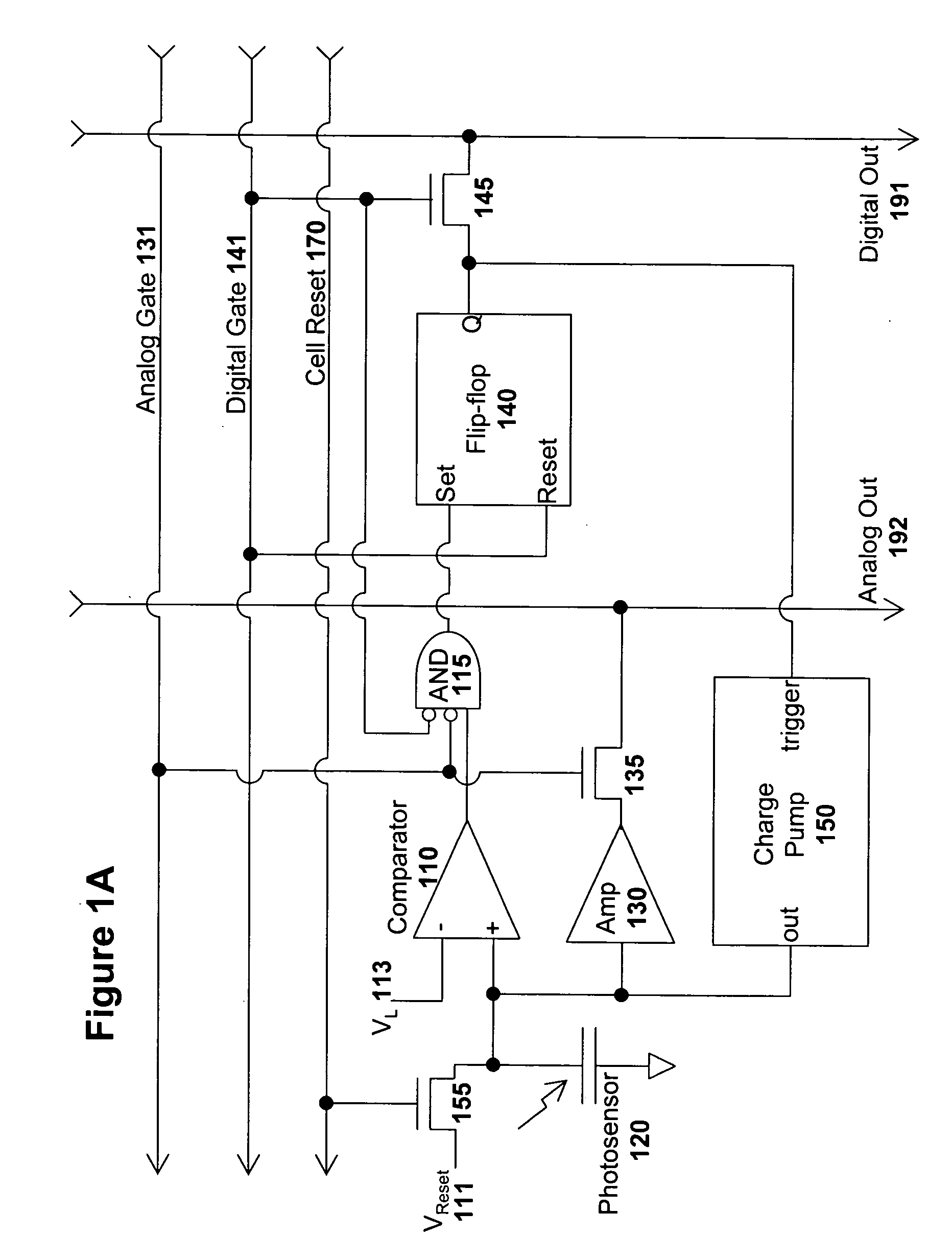
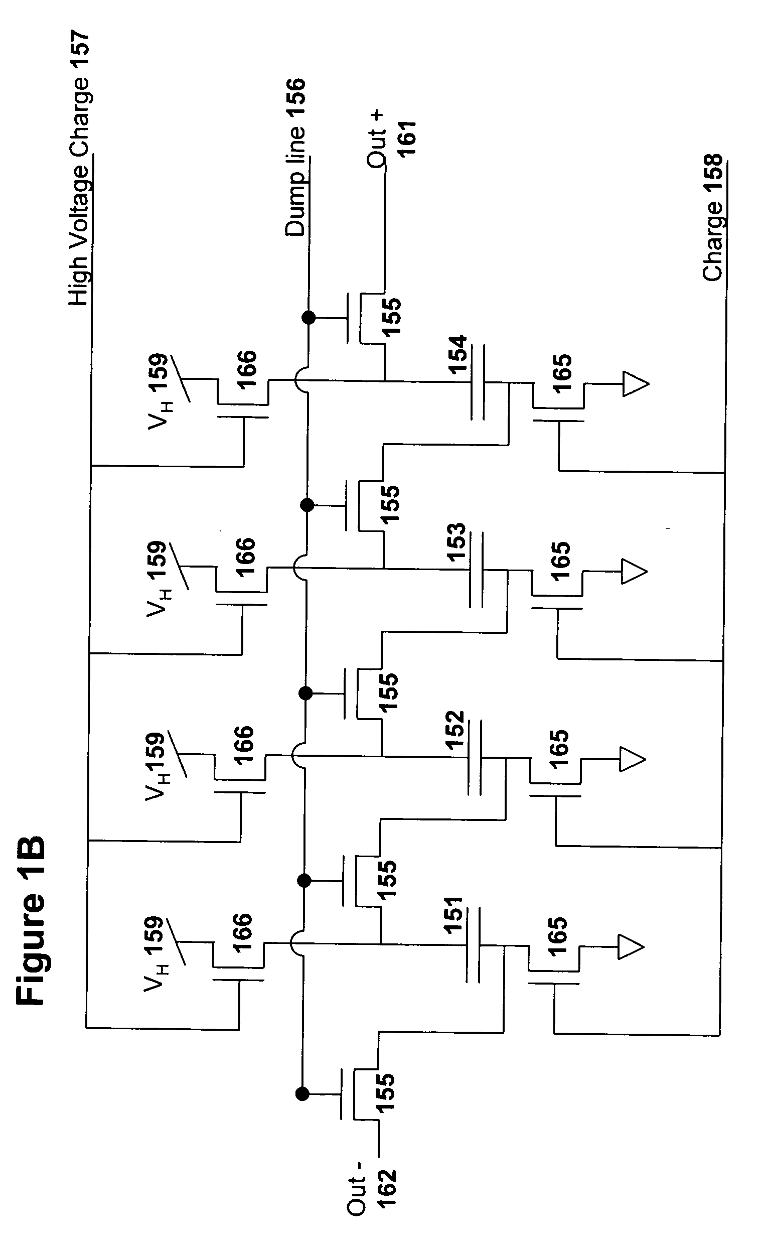
[0023] Electronic pixel sensor apparatuses and methods and for constructing those electronic pixel sensor apparatuses are disclosed. In the following description, for purposes of explanation, specific nomenclature is set forth to provide a thorough understanding of the present invention. However, it will be apparent to one skilled in the art that these specific details are not required in order to practice the present invention. For example, the electronic pixel sensor apparatuses have been described with reference to the industry standard Complementary Metal-Oxide-Semiconductor (CMOS) manufacturing process. However, the same designs may be implemented with other electronic manufacturing processes. Furthermore, the present invention is described with reference to photo sensors. However, any other type of sensor circuit that generates current may be used.

Dynamic Range Extended CMOS Pixel Sensor Design

[0024] As previously set forth, existing CMOS pixel sensor circuit designs use a p...


PUM


Abstract

The dynamic range of existing CMOS image sensors is limited. The present invention introduces an extended dynamic range CMOS pixel sensor circuit. The extended dynamic range CMOS pixel sensor circuit is relatively similar to existing CMOS pixel sensors except that a charge pump has been added to recharge the pixel sensor when the pixel sensor is nearing charge depletion. Every firing of the charge pump is counted. To create a final output for the extended dynamic range CMOS pixel sensor circuit, the number of charge pump firings is combined with a final analog voltage reading of the pixel sensor circuit.

Description

FIELD OF THE INVENTION [0001] The present invention relates to the field of electronic image sensor devices. In particular the present invention discloses novel CMOS based electronic pixel sensor designs. BACKGROUND OF THE INVENTION [0002] Most early electronic pixel sensor devices are charge-coupled devices (CCD). A CCD pixel sensor is a semiconductor device that is sensitive to light. A CCD pixel sensor consists of a two-dimensional array of individual pixels that each capture a charge caused by photons striking the pixel element. As more photons strike a pixel, the more of charge is created such that the charge is proportional to the intensity of light striking the pixel. [0003] CCD pixel sensors have been used to capture high-quality images. However, CCD pixel sensors are not manufactured with the industry standard Complementary Metal-Oxide-Semiconductor (CMOS) manufacturing processes used to create most digital integrated circuits. Thus, separate semiconductor parts were needed...

Claims


Application Information

Patent Timeline
Patent Type & Authority Applications(United States)
IPC IPC(8): H01J40/14
CPCH01L27/14643H01L27/14689H04N3/155H04N25/772
Inventor PETING, MARK
Owner PETING MARK
Why Eureka
Try Eureka