Frame-shuttered CMOS image sensor with simultaneous array readout

a cmos image sensor and array readout technology, applied in the field of frame shuttered cmos image sensor with simultaneous array readout, can solve the problems of high cost, insufficient scale, and high cost of foundries using specialized and expensive processes, and achieve the effect of low cost and low cos

Active Publication Date: 2007-09-25
FORZA SILICON
View PDF4 Cites 10 Cited by
  • Summary
  • Abstract
  • Description
  • Claims
  • Application Information

AI Technical Summary

Benefits of technology

[0022]This invention eliminates the drawbacks of the rolling shutter, while avoiding the use of the in-pixel capacitors of the pixel-shuttered approach. We call this invention the “Simultaneous Array Readout”. In this invention, a larger number of he storage capacitors are brought to the edges of the array. Unlike the rolling shutter scheme, where the number of capacitor pairs is equal to the number of columns in the array, for Simultaneous Array Readout the number of capacitor pairs is equal to the number of pixels in the array. This allows the array to be read out in a fully parallel fashion, which enables the implementation of a full frame-shutter without the requirement for a pixel with in-pixel storage.
[0024]1) Minimal image blurring—The entire array is read out simultaneously, minimizing distortions in the image.
[0027]4) Use of low cost fabrication process—This invention can be (and has been) implemented in a low cost digital process.
[0028]An additional benefit of the Simultaneous Array Readout scheme is that there is no longer a requirement to address the array on a row-by-row basis. This means that there is no need for the row decoder logic present in both the frame-shutter and rolling-shutter schemes.

Problems solved by technology

The biggest problem with CCD's is that there aren't enough economies of scale.
They are created in foundries using specialized and expensive processes that can only be used to make other CCD's.
Using this same process and the same equipment to manufacturer CMOS image sensors cuts costs dramatically because the fixed costs of the plant are spread over a much larger number of devices.
As a result of these economies of scale, the cost of fabricating a CMOS wafer is one-third the cost of fabricating a similar wafer using a specialized CCD process.
Early versions of CMOS image sensors were plagued with noise problems, and used mainly in low-cost cameras.
1) Charge transfer—it is difficult to do an efficient and noiseless charge transfer from the photo-sensing node to the storage capacitor in a fabrication process not specially modified for image sensor applications. With the components available in typical prior art arrays, the charge must be shared between the detection node and storage node during read out. A significant part of the signal charge is lost during this process.
2) Readout noise—The use of the storage node as a shutter precludes the use of correlated double sampling (CDS) in this readout method. In CDS, a reference signal is stored in the storage node. By comparing this reference to the signal value, the pixel readout noise is significantly reduces. However, CDS is not compatible with a pixel shutter.
3) Reduction in input signal—the in-pixel capacitor, which is opaque, reduces the overall pixel area dedicated to the collection of light.
1) Image blur—the movement in the scene is seen differently by each row in the array, since each row has a different integration start and stop time as indicated in FIG. 4. For example, if the sensor is moving sideways with respect to a vertical bar, the bar will appear bent in the image due to the staggered integration times of each row. FIG. 5 shows this image artifact.
2) Power consumption—to reduce the effects of image blur, the frame rate for a rolling shutter sensor must be greatly increased. The higher frame rate significantly increases the power consumption of the sensor.
3) Readout noise—the kTC noise from the reset operation of the pixel is not cancelled, because the reset that starts the integration is not the same as the reset used to subtract from the signal level.
The most critical problem faced by an image sensor in recording high-speed motion is that of image blur.
In these applications, the available power is typically quite limited by the interface standard.
However, the illumination sources output can not be increased without increasing the power consumption of the system.
The optical mouse is used in extremely cost sensitive markets.

Method used


Image

  • Frame-shuttered CMOS image sensor with simultaneous array readout
  • Frame-shuttered CMOS image sensor with simultaneous array readout
  • Frame-shuttered CMOS image sensor with simultaneous array readout

Examples


Embodiment Construction

Simultaneous Array Readout

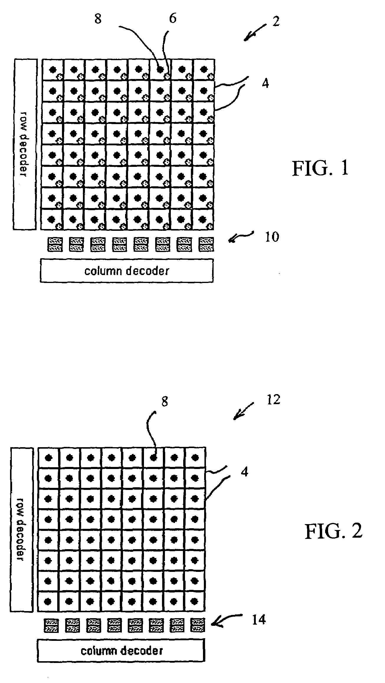
[0035]FIG. 6 shows a possible implementation of our Simultaneous Array Readout. This is an 8×8 pixel array 16 useful as a very high-speed, very low-cost optical sensor useful for applications such as the sensor in an optical mouse for a personal computer or a video game. Individual pixels are indicated at 4 and the pixel photodiode sensitive region is shown at 6. Preferred locations of signal readout and reset circuitry are shown at 18. Locations of column decoders are shown at 20.

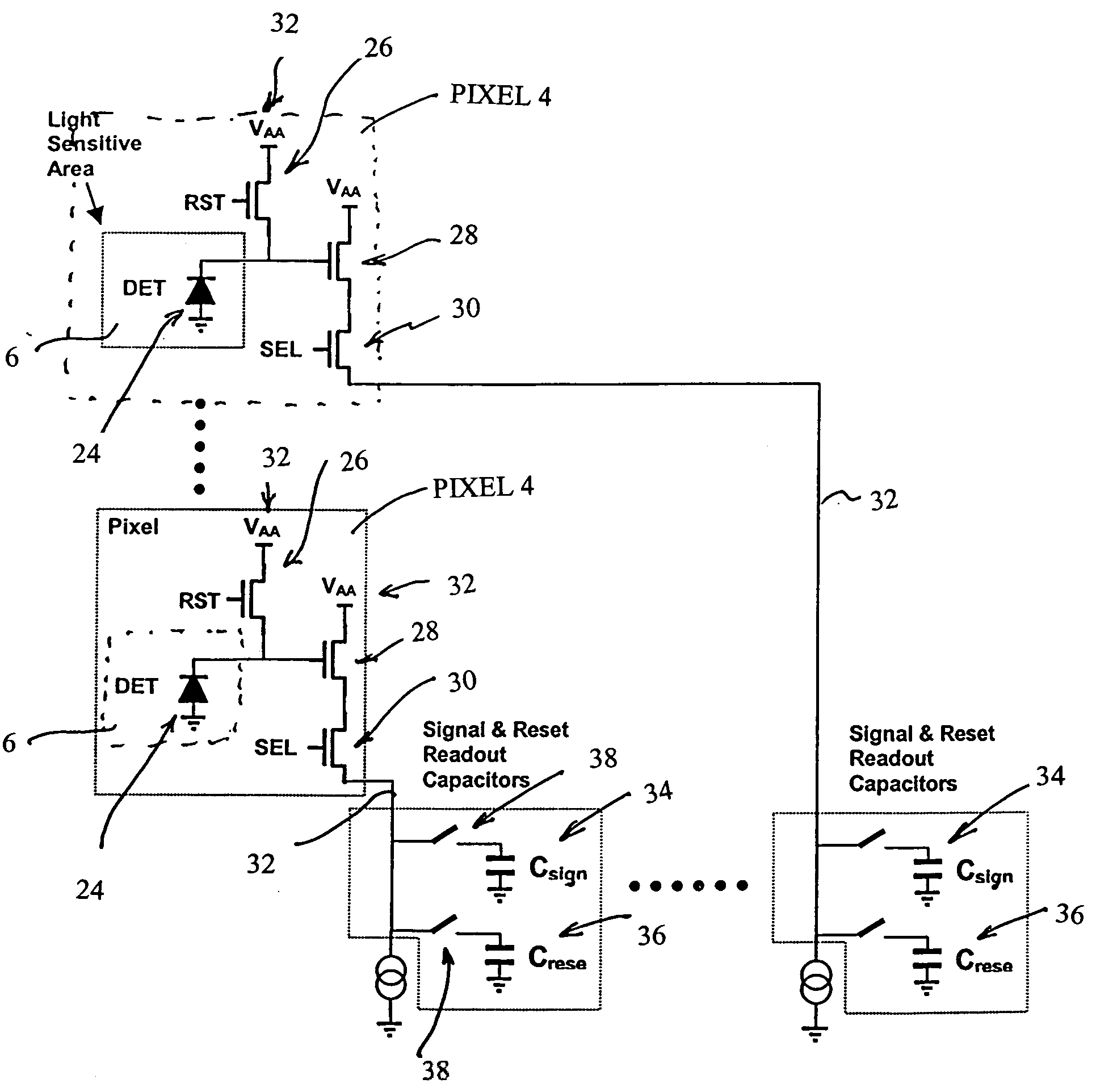
[0036]FIG. 7 shows a preferred implementation of this architecture in schematic form. For this example, an 8 by 8 pixel array 16 is indicated. Two pixels 4 of the array are shown in schematic detail and the other 62 pixels are represented by dots. Each pixel includes a light sensitive region 6 formed with a PIN diode junction 24. Each pixel also includes a reset transistor (RST) 26 that is operated by the application of a reset signal at the gate of the transistor to apply a reset...


PUM


Abstract

A frame shuttered CMOS image sensor with simultaneous array readout. An array of CMOS pixels are printed on a silicon substrate. Within each pixel is a light sensitive region comprising a photo sensitive diode for converting photons into electrical charge and at least three transistors to permit reading of reset electrical charges and collected electrical charges and for re-setting the photosensitive diode. The sensor includes an array of signal and re-set readout capacitors located on the substrate but outside of the pixel array. Metal conductors printed in said substrate connect each pixel in said pixel array with a signal capacitor and a re-set capacitor in array of signal and re-set readout capacitors. Transistor switches printed in said substrate but outside of said pixel array are used to isolate the signal and re-set capacitors from each other and from the pixels. Control circuitry is provided for re-setting simultaneously each of the pixels in the pixel array, for collecting simultaneously re-set signals from each pixel on to one of the reset capacitors in the array of readout capacitors and for collecting simultaneously integrated pixel signals from each pixel on to one of the signal capacitors in the array of readout capacitors. Readout circuitry is provided for reading charges collected on the array of signal and re-set capacitors.

Description

[0001]This application claims the benefit of provisional Application, Ser. No. 60 / 481,149, filed Jul. 28, 2003. This invention relates to CMOS image sensors and in particular to high-speed array readout CMOS image sensors.BACKGROUND OF THE INVENTION[0002]Until recently, charge-coupled devices (CCD's) were the only image sensors widely used in digital imaging. They have been well developed through their use in astronomical telescopes, scanners, and video camcorders. However, CMOS image sensors promises to eventually become the image sensor of choice in a large segment of the digital imaging market. Both CCD and CMOS image sensors capture light on a grid of small pixels on their surfaces. It's how they process the image and how they are manufactured where they differ from one another. CCD Image Sensors[0003]CCD's got their name from the way the charges on the pixels are read after an exposure. After the exposure the charges on the first row are transferred to a place on the sensor cal...

Claims


Application Information

Patent Timeline
Patent Type & Authority Patents(United States)
IPC IPC(8): H01J1/42H01J40/14H01L31/00H01L31/062H04N3/14H01L27/00H01L27/146H04N3/15
CPCH01L27/14643H04N5/3532H04N5/3575H04N25/531H04N25/616
Inventor HUANG, STEVEN LEIVAN BLERKOM, DANIEL ALAN
Owner FORZA SILICON
Why Eureka
Try Eureka