

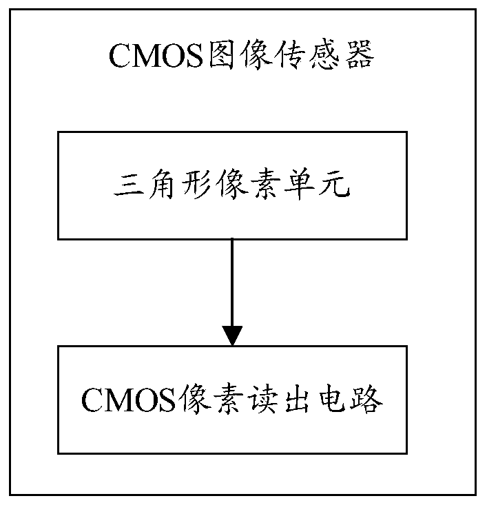
CMOS image sensor, image processing method and storage medium
An image sensor and pixel technology, which is applied in the field of image processing and can solve the problems of low pixel density and low pixel unit arrangement density of CMOS image sensors.
- Summary
- Abstract
- Description
- Claims
- Application Information
AI Technical Summary
Problems solved by technology
Method used
Image


Examples
Embodiment 1
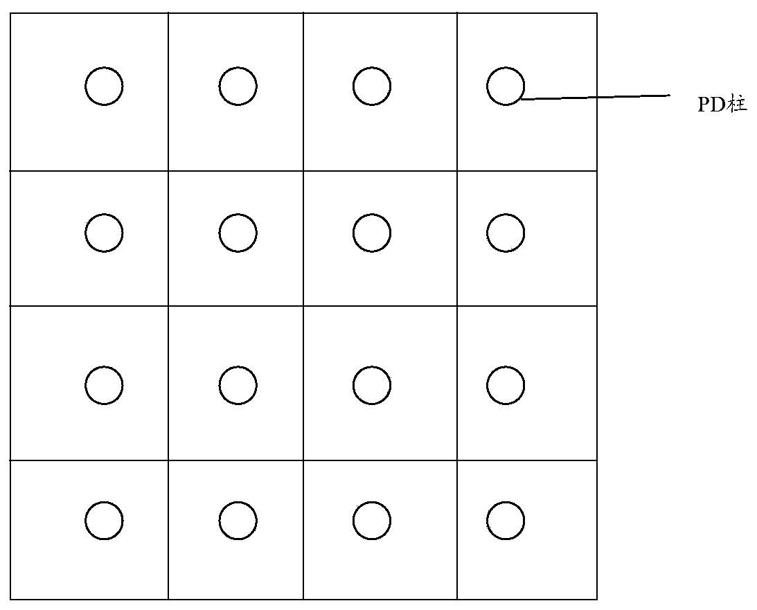
[0035] The embodiment of the present application provides a CMOS image sensor, such as figure 2 As shown, the CMOS image sensor includes:
[0036] A triangular pixel unit arranged in a hexagonal array, the triangular pixel unit is provided with a photodiode PD column, and the triangular pixel unit absorbs RGB monochromatic light by using the PD column, and converts the corresponding optical signal into an electrical signal;
[0037] The CMOS pixel readout circuit connected to the triangular pixel unit is used to amplify the electrical signal and read out the electrical signal.
[0038] A CMOS image sensor provided in an embodiment of the present application is suitable for collecting optical signals and performing image processing on the collected optical signals to obtain images corresponding to the optical signals.
[0039] In the embodiment of the present application, the CMOS image sensor is composed of a pixel unit circuit and a CMOS circuit, wherein the pixel unit circ...
Embodiment 2
[0071] An embodiment of the present application provides an image processing method, which is applied to a CMOS image sensor composed of triangular pixel units arranged in a hexagonal array and a CMOS pixel readout circuit. The triangular pixel units are provided with photodiode PD columns, such as Figure 6 As shown, the method includes:
[0072] S101. Use the PD column to absorb RGB monochromatic light, and convert the corresponding optical signal into an electrical signal.
[0073] An image processing method provided in an embodiment of the present application is applicable to a scenario where a CMOS image sensor is used to collect an optical signal, and the collected optical signal is subjected to image processing to obtain an image corresponding to the optical signal.
[0074] In the embodiment of the present application, the CMOS image sensor is composed of a pixel unit circuit and a CMOS circuit, wherein the pixel unit circuit is used to convert the collected optical si...
Embodiment 3
[0098]An embodiment of the present application provides a storage medium on which a computer program is stored. The computer-readable storage medium stores one or more programs. The one or more programs can be executed by one or more processors and applied to pixel In the unit circuit, the computer program realizes the image processing method described in the second embodiment.
[0099] Specifically, when the program instructions corresponding to an image processing method in this embodiment are read or executed by an electronic device, the following steps are included:
[0100] Use the PD column to absorb RGB monochromatic light, and convert the corresponding optical signal into an electrical signal;
[0101] The electrical signal is amplified by the CMOS pixel readout circuit, and the electrical signal is read out.
[0102] In the embodiment of the present invention, further, the hexagonal array of the triangular pixel units is arranged such that six triangular pixel units ...
PUM
 Abstract
Description
Claims
Application Information