Device and method for detecting organic molecules in a test substance

a technology of organic molecules and devices, applied in the field of apparatus and a method for detecting organic molecules, can solve the problems of high cost, mechanical vulnerability, large size, etc., and achieve the effects of improving the regeneration ability of the test system, reducing the measurement time, and increasing the sensitivity

Inactive Publication Date: 2006-05-16
LOSSAU HARALD
View PDF22 Cites 34 Cited by
  • Summary
  • Abstract
  • Description
  • Claims
  • Application Information

AI Technical Summary

Benefits of technology

[0016]To be able to supply the probe substance to the biochip, a supply apparatus is employed. Both independent supply apparatuses, especially syringes, pipettes, tubing, cannula, piping, and funnels, and apparatuses connected with the test system may be considered. The latter can be integrated into the casing of the test system and can effect protection of the test system from interference factors such as impurities, mechanical stress, temperature differences, and evaporation, as well as facilitate sparing use of the probe substance.Illumination System
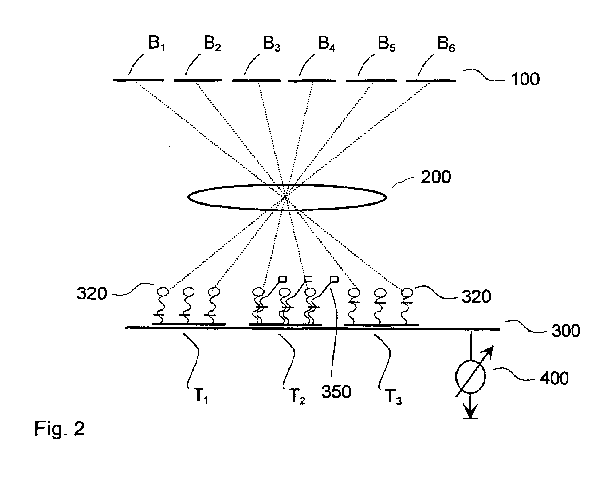
[0025]For the biochips with electrical readout that are particularly preferably employed as the test system, especially DNA chips with direct electrical readout (especially based on patent applications DE 19921940, DE 19926457, and DE 19945398) the detection system preferably comprises a measuring device for determining the electrical communication between the test sites and the conductive surface of the biochip. This measuring device is preferably a current, charge, voltage, or potential measuring device, a cyclovoltammetry device, an amperometry device, or a conductivity measuring device. A cyclovoltammetry device is a measuring device for recording current-voltage curves, the voltage being changed periodically and linearly with time. An amperometry device is a measuring device for recording current-time curves. A conductivity measuring device allows conductivity to be measured, especially by measuring the current at a fixed voltage or by measuring the voltage at a constant current. Biochips with microelectrodes allow spatial limitation of the electrical readout and thus spatial resolution of the measurement, or an electrical readout limited to individual test sites.
[0029]In this case, the illumination system is dimensioned such that only part of the photosensitive biochip is illuminated. In a first step, initially this part of the chip is excited and read out. In a subsequent step, either the chip is moved the width of one field via an x-y translation table or the illumination field is moved the width of one field via movable tilted mirrors. Thereafter, the chip region thus newly selected is excited and read out. This process is repeated until the entire chip has been read out. In the case of an illumination system consisting of an array having a limited number of pixels, illumination of the entire chip can be achieved with high pixel density through combination with a scanning process.
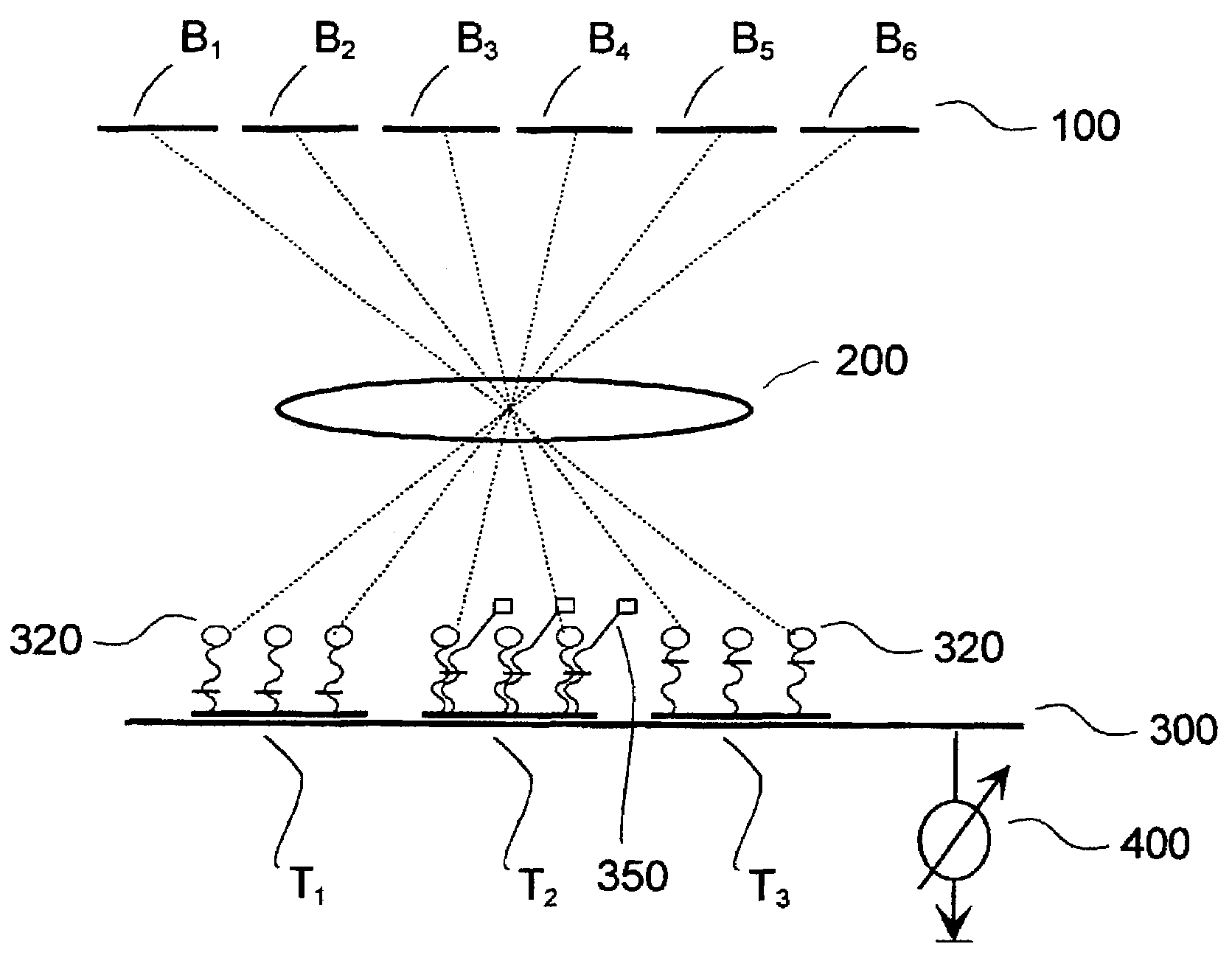
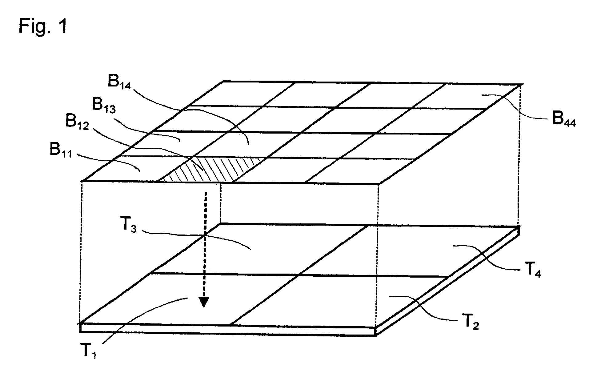
[0038]While in the case of scanning illumination methods according to the prior art, for example employing a laser scanner, typically only one test site can be illuminated at a time, the illumination system described within the context of the present invention allows illuminating multiple test sites simultaneously. As a result, there are a number of illumination patterns to select from. For the detection method described here, an optimum illumination pattern adjusted to the conditions of the detection apparatus can be selected. In particular, multiple test sites, preferably those for which the probability of a reaction with the organic molecules to be detected is low, can first be simultaneously illuminated and read out. If no reaction is detected within such a group, a reaction can be precluded for the entire group and further readout of the individual test sites of this group can be dispensed with. Only if a reaction was ascertained within such a group of test sites, or could not be reliably precluded, is a further illumination and readout of these test sites necessary in a subsequent step, in a different grouping or individually. Since, in the case of such a procedure, entire groups of test sites are in some cases read out simultaneously and can be classified as non-reacting, the overall readout process time can be shortened. For example, in the case of a chip having N=2n test sites (n is an integer) for which a reaction with the test solution is detectable at only one test site, instead of N readout steps, only 2n+1 readout steps are necessary if the following readout method is applied: First, all test sites are read out at once, then each half thereof, and thereafter, the half in which a reaction was detected is, in turn, divided into two halves, both of which are read out, the half in which a reaction was detected being iteratively halved until, finally, the test site at which a reaction is detectable is unambiguously identified. In this example, time savings by a factor of N / (2n+1) are also possible, in the case of a chip with 1024 test sites for example, time savings by a factor of 49. If a reaction is detectable at multiple test sites, the time savings are less, since the iteration process must branch.
[0042]In addition to an increase in sensitivity and / or a reduction of the measuring time, a further advantage of periodic illumination and readout of the test sites is improved regeneration ability of the test system. For example, undesired intermediate states produced by optical excitation, especially triplet states of the probes, targets, or other molecules in the vicinity of the test site just addressed, can relax to the normal state in the dark phase. Regeneration can also consist in possible substances converted by the readout process, especially in the vicinity of the test site, especially ions in the case of an electrical readout process, being removed or delivered subsequently.

Problems solved by technology

Other optical readout systems, such as that described in WO09947964A1, are based on movable optical components, which make the construction expensive and / or susceptible to interference.
Disadvantages of all known scanning systems are that they are mechanically vulnerable, relatively large, and expensive.

Method used


Image

  • Device and method for detecting organic molecules in a test substance
  • Device and method for detecting organic molecules in a test substance
  • Device and method for detecting organic molecules in a test substance

Examples


embodiment 1

[0046]FIG. 3 shows schematic diagrams of exemplary embodiments according to the present invention, wherein a liquid crystal display (LCD) is used for the illumination system (Embodiment 1).

[0047]FIGS. 3A to 3C show apparatuses in which, in addition to illumination optics, a projection system is employed (Embodiment 1a).

[0048]FIGS. 3D and 3E show more simply constructed apparatuses with no projection system, in which the biochip is arranged very near the liquid crystal (Embodiment 1b).

[0049]FIG. 3A shows an exemplary embodiment according to the present invention, with LCD, projection system, and electrical detection.

[0050]FIG. 3B shows an exemplary embodiment according to the present invention, with LCD, projection system, and optical detection by means of beam splitters.

[0051]FIG. 3C shows an exemplary embodiment according to the present invention, with LCD, projection system, and optical detection (non-collinear).

[0052]FIG. 3D shows an exemplary embodiment according to the present ...

embodiment 2

[0054]FIG. 4 shows schematic diagrams of exemplary embodiments according to the present invention, wherein a digital micromirror device (DMD) is used for the illumination system (Embodiment 2).

[0055]FIG. 4A shows an exemplary embodiment according to the present invention, with DMD, projection system, and electrical detection.

[0056]FIG. 4B shows an exemplary embodiment according to the present invention, with DMD, projection system, and optical detection by means of beam splitters.

[0057]FIG. 4C shows an exemplary embodiment according to the present invention, with DMD, projection system, and optical detection (non-collinear).

embodiment 3

[0058]FIG. 5 shows schematic diagrams of exemplary embodiments according to the present invention, wherein a video projector is used for the illumination system (Embodiment 3).

[0059]FIG. 5A shows an exemplary embodiment according to the present invention, with video projector, projection system, and electrical detection.

[0060]FIG. 5B shows an exemplary embodiment according to the present invention, with video projector, projection system, and optical detection by means of beam splitters.

[0061]FIG. 5C shows an exemplary embodiment according to the present invention, with video projector, projection system, and optical detection (non-collinear).


PUM

PropertyMeasurementUnit
threshold frequencyaaaaaaaaaa

Abstract

An apparatus for detecting organic molecules, especially biomolecules and polymers, in a probe substance, comprisesa test system (300) comprising an array of test sites (T) to which the probe substance can be supplied, each test site having specific probe molecules (320), an illumination system (100) for optically illuminating a sub-array of test sites (T), and a detection system (400) for identifying those test sites (T) whose probe molecules (320) interact with the organic molecules (350) to be detected, the illumination system (100) comprising an array of independently addressable illumination sources (B) arranged such that to each test site (T) of the sub-array is assigned at least one illumination source (B) that illuminates substantially only it.

Description

FIELD OF THE INVENTION[0001]The present invention relates to an apparatus and a method for detecting organic molecules, especially biomolecules and polymers, in a probe substance.BACKGROUND OF THE INVENTION[0002]Biochips are used particularly in the DNA chip and protein chip embodiments in biotechnology and genetic research. They are ascribed great potential in medical diagnostics, pharmacological and toxicological test procedures, and in the agricultural sector.[0003]A biochip typically includes a two-dimensional array of regions having organic molecules (probes) that are immobilized on a surface and that can specifically react with chemical substances comprising a probe substance (targets). The objective here is the parallel detection of many interactions between probes and targets. When illuminated, photosensitive biochips exhibit a physical reaction that specifically depends on the interaction between probes and targets.[0004]Detection of these interactions occurs, for example, ...

Claims


Application Information

Patent Timeline
Patent Type & Authority Patents(United States)
IPC IPC(8): G01N21/64B01J19/00C12Q1/68C12Q1/6837C40B40/06C40B40/10C40B40/18C40B60/14G01N27/06G01N27/26G01N27/416G01N27/42G01N33/53G01N37/00
CPCG01N21/6452B01J2219/00434B01J2219/00605B01J2219/00608B01J2219/00659B01J2219/00707B01J2219/00722B01J2219/00725B01J2219/00729B01J2219/00745B01J2219/0075C12Q1/6837C40B40/06C40B40/10C40B40/18C40B60/14B01J2219/00439
Inventor HARTWICH, GERHARDLOSSAU, HARALD
Owner LOSSAU HARALD
Why Eureka
Try Eureka