Flash memory

a flash memory and flash memory technology, applied in the field of flash memory devices, can solve the problems of limiting hindering the integration of the device, and further increasing the area between the control gate and the floating gate, so as to increase the gate couple ratio and the effect of the device integration

Active Publication Date: 2006-08-10
POWERCHIP SEMICON MFG CORP
View PDF12 Cites 6 Cited by
  • Summary
  • Abstract
  • Description
  • Claims
  • Application Information

AI Technical Summary

Benefits of technology

[0008] Accordingly, the present invention provides a flash memory device and a fabrication method thereof for increasing the gate couple ratio and the integration of the device.
[0014] Since according to the fabrication method for a flash memory device of the present invention, the floating gate is curved, the area between the floating gate and the control gate of the flash memory device is greater compared to that of the conventional stacked-gate flash memory device. Therefore, the gate couple ratio between the floating gate and the control gate is increased. Further, two memory cells is formed in one memory unit according to the present invention, and the two memory cells share one control gate. The level of integration of the device can thereby improve.
[0021] Since one side of each floating gate of the flash memory device of the invention is curved, the area between the floating gate and the control gate of the flash memory device of the present invention is greater compared to that of the conventional stacked gate flash memory device. The gate-couple ratio between the floating gate and the control gate is thereby increased to raise the efficiency of the device.

Problems solved by technology

However, due to the limitations inherent in the manufacturing process, for example, the patterning process for the control gate and the floating, to further increase the area between the control gate and the floating gate is restricted.
Consequently, to increase the level of integration of the device is thereby hindered.

Method used


Image

  • Flash memory
  • Flash memory
  • Flash memory

Examples


Embodiment Construction

[0028] Reference will now be made in detail to the present preferred embodiments of the invention, examples of which are illustrated in the accompanying drawings. Wherever possible, the same reference numbers are used in the drawings and the description to refer to the same or like parts.

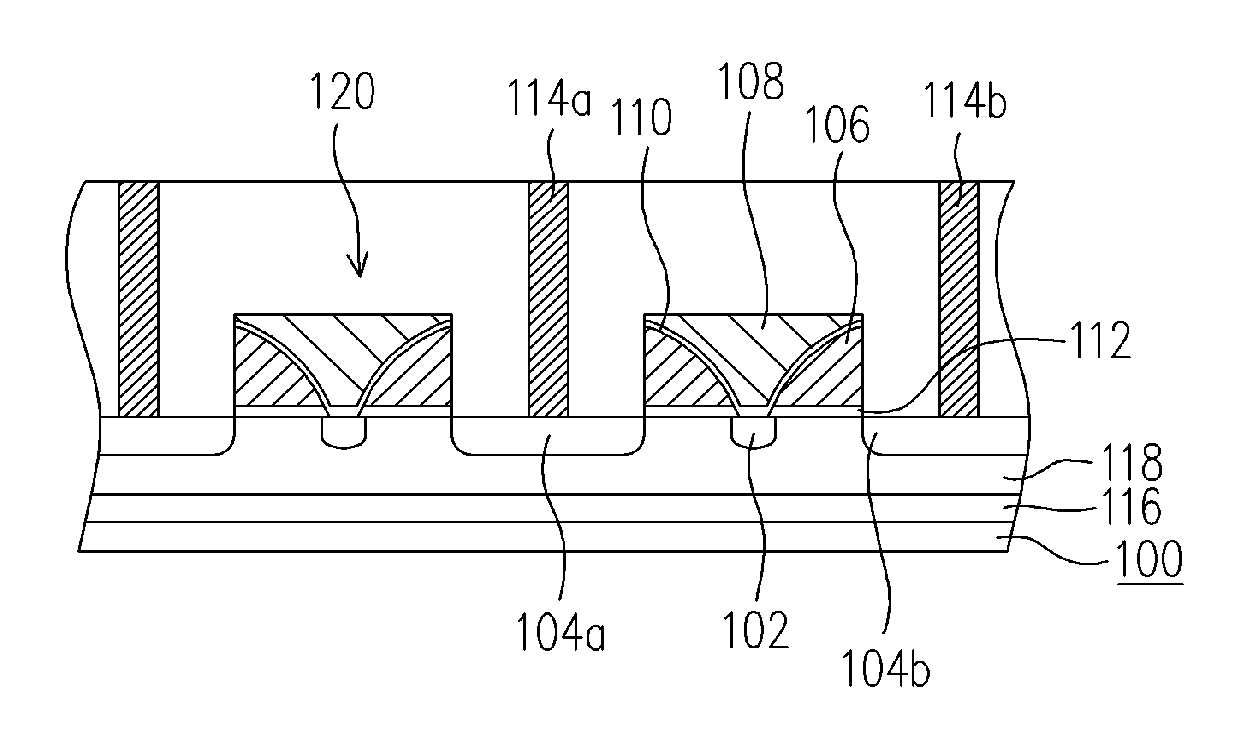
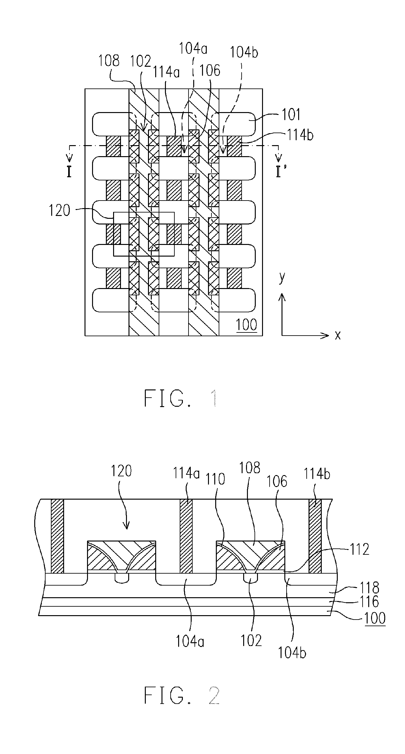
[0029]FIG. 1 is a schematic, top view of a portion of a flash memory device according to one embodiment of the present invention. FIG. 2 is a cross-sectional view of FIG. 1 along the cutting line I-I′ (X-direction).

[0030] Referring concurrently to FIGS. 1 and 2, the flash memory device includes a substrate 100, a plurality of buried doped regions 102, a plurality of source regions 104a, a plurality of drain regions 104b, a plurality of floating gates 106, a plurality of control gates 108, a plurality of inter-gate dielectric layers 110, a plurality of tunneling dielectric layer 112. In this embodiment, the flash memory device of the present invention further includes a plurality of source region c...


PUM


Abstract

A method for fabricating a flash memory is described. A mask layer having openings to expose a portion of the substrate is formed on the substrate. A tunneling dielectric layer is formed at the bottom surface of the openings. Conductive spacers are formed on the sidewalls of the openings. The conductive spacers are patterned to form a plurality of floating gates. A plurality of buried doped regions is formed in the substrate under the bottom surface of the openings. An inter-gate dielectric layer is formed over the substrate. A plurality of control gates is formed over the substrate to fill the openings. The mask layer is removed to form a plurality of memory units. A plurality of source regions and drain regions are formed in the substrate beside the memory units.

Description

CROSS-REFERENCE TO RELATED APPLICATION [0001] This application claims the priority benefit of Taiwan application serial no. 94103556, filed on Feb. 4, 2005. All disclosure of the Taiwan application is incorporated herein by reference. BACKGROUND OF THE INVENTION [0002] 1. Field of the Invention [0003] The present invention relates to a memory device. More particularly, the present invention relates to a flash memory device and a fabrication method thereof. [0004] 2. Description of Related Art [0005] Electrically erasable programmable read only memory (EEPROM) is a type of non-volatile memory that allows multiple data reading, writing and erasing operations. In addition, the stored data will be retained even after power to the device is removed. With these advantages, electrically erasable programmable read only memories have been broadly applied in personal computers and electronic equipment. [0006] A floating gate and a control gate of a typical flash memory device are fabricated w...

Claims


Application Information

Patent Timeline
Patent Type & Authority Applications(United States)
IPC IPC(8): H01L29/788H01L21/336
CPCH01L27/115H01L27/11521H01L29/7782H10B69/00H10B41/30
Inventor PAN, JUI-YUHSU, CHENG-YUANCHUANG, I-CHUNHUNG, CHIH-WEI
Owner POWERCHIP SEMICON MFG CORP
Why Eureka
Try Eureka