Pattern forming method and method of manufacturing semiconductor device

a technology of semiconductor devices and forming methods, which is applied in the direction of originals for photomechanical treatment, instruments, photomechanical equipment, etc., can solve the problems of affecting the imaging performance, the optical path length, and the aberration of a projected image, so as to achieve the effect of avoiding the effect of affecting the operation of tools

Inactive Publication Date: 2006-08-10
KK TOSHIBA
View PDF1 Cites 40 Cited by
  • Summary
  • Abstract
  • Description
  • Claims
  • Application Information

AI Technical Summary

Problems solved by technology

This arises from the fear that a photo-acid generator contained in the resist film and its photoproducts which are photo-generated acids, basic materials and other low-molecular components elute into the immersion fluid and contaminate the element of the projection optics which contacts with the liquid immersion fluid, a shower head, a wafer stage, and so forth.
On the other hand, the elusion of the substance into the immersion fluid changes the refractive index of the immersion fluid and thus changes the optical path length, which causes aberration of a projected image and affects the imaging performance.
Furthermore, in an immersion lithography exposure tool which selectively fills the liquid immersion fluid between a downstream surface of an optical axis of the objective lens and a substrate upper surface targeted for image projection, the following problems occur in a case where the liquid immersion fluid remains on the substrate when the substrate is loaded after completion of an exposure step.
If the liquid immersion fluid leaks into the exposure tool and a coating tool and touches electric systems therein, trouble occurs in the operation of the tools.
This results in a reduction in productivity and generation of costs due to the stoppage and repair of the tools, and a loss due to the reprocessing and damage of a wafer.
This leads to a decrease in productivity due to deterioration of lithographic performance, stops the tools and generates repair cost.
This results in a productivity decrease.
As a result, adherents on the inner wall of a baking unit in the PEB step increase, and the adherents act on a wafer as dust to cause a pattern defect, leading to a productivity decrease and a loss.
This causes the removal of the cover film, an insufficient removal of the cover film due to occurrence of parts of different development characteristics, or a loss from a productivity decrease due to occurrence of development defects.

Method used


Image

  • Pattern forming method and method of manufacturing semiconductor device
  • Pattern forming method and method of manufacturing semiconductor device
  • Pattern forming method and method of manufacturing semiconductor device

Examples


first embodiment

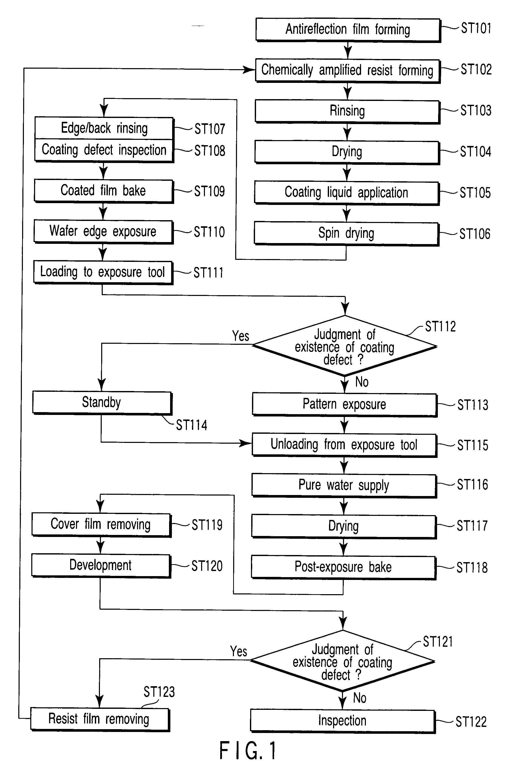
[0058]FIG. 1 shows a flowchart to explain a pattern forming method of a semiconductor device according to a first embodiment of the present invention.

[0059] First, a bottom-layer antireflection film is formed on a semiconductor substrate. In the present embodiment, for example, a coating-type bottom-layer antireflection film is formed (step ST101).

[0060] Then, a chemically amplified positive resist film is formed on the antireflection film (step ST102). In forming the resist film, the resist film at the edge of a wafer is selectively removed.

[0061] In a separately conducted surface analysis of some ArF chemically amplified resist films, it has been proved that photo-acid generators and acid trap agents (such as amine) are distributed on the film surface. In order to remove the photo-acid generators and the acid trap agents on the resist film surface, pure water is supplied to the resist for rinsing (step ST103). This rinsing removes the photo-acid generators and the acid trap age...

second embodiment

[0110] In the present embodiment, an example will be described in which a coating defect inspection is conducted after a substrate is loaded to an exposure tool.

[0111]FIG. 13 is a flowchart to explain a method of forming a resist pattern according to the second embodiment of the present invention.

[0112] As in the first embodiment, processing from step ST201 to step ST206 is similar to that from step ST101 to step ST110 described in the first embodiment referring to FIG. 1, and therefore duplicated explanation is omitted.

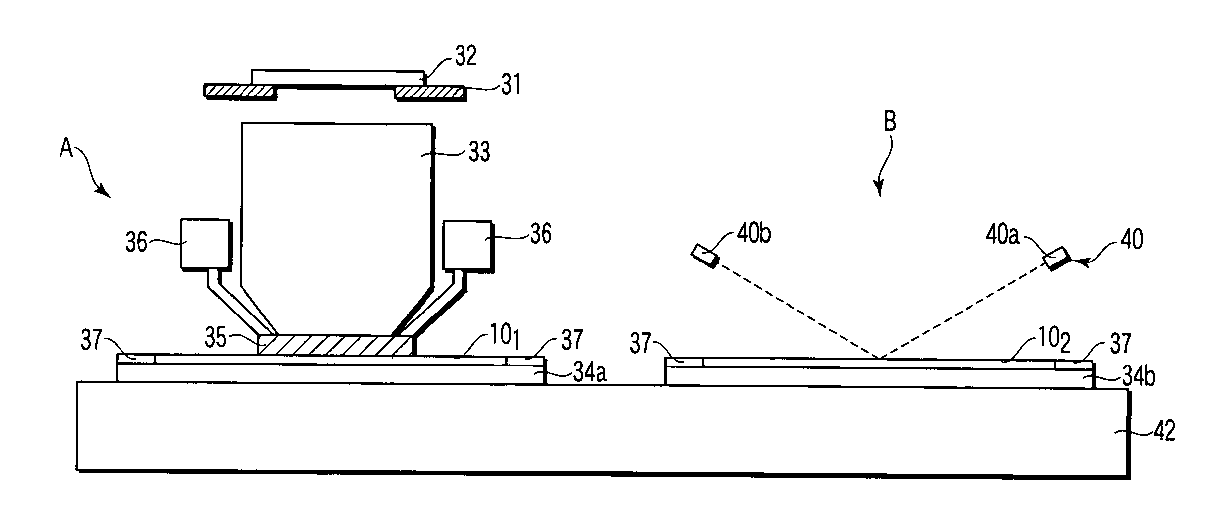
[0113] Then, the substrate is loaded to the exposure tool (step ST207). In recent years, a twin-stage type exposure tool equipped with two stages to hold the substrate has appeared. The exposure tool used in the present embodiment is schematically described referring to FIG. 14. FIG. 14 is a diagram schematically showing the exposure tool according to the second embodiment of the present invention.

[0114] The twin-stage type exposure tool comprises first and secon...

third embodiment

[0125]FIG. 15 is a flowchart to explain a manufacturing process of a semiconductor device according to a third embodiment of the present invention.

[0126] First, an antireflection film is formed on a semiconductor substrate. In the present embodiment, for example, a coating-type antireflection film is formed (step ST301). Then, a chemically amplified positive resist film is formed on the antireflection film (step ST302). A cover film is formed on the resist film (step ST303). Wafer edge exposure is conducted (step ST304). The wafer is loaded to an immersion lithography scan and repeat type exposure tool (step ST305). After various alignments are made, a semiconductor device pattern is transferred by immersion lithography to form a latent image in the resist film (step ST306).

[0127] Then, an inspection is conducted to know whether or not a liquid immersion fluid used during the immersion lithography remains on the cover film (step ST307). As detection mechanisms of the residual liqu...


PUM

PropertyMeasurementUnit
refractive indexaaaaaaaaaa
shrinkageaaaaaaaaaa
refractive indexaaaaaaaaaa

Abstract

A pattern forming method includes forming a resist film on a substrate, coating the resist film with a coating solution which forms a cover film on the resist film to form the cover film on the resist film, transferring a pattern onto the resist film by an immersion lithography method using a liquid immersion fluid to form a latent image on the resist film, removing the cover film after the formation of the latent image, conducting a first inspection to inspect whether or not the cover film has a defect between said forming the latent image and said removing the cover film, performing predetermined processing when the defect is found in the first inspection, and developing the resist film to form a resist pattern on the substrate after said removing the cover film.

Description

CROSS-REFERENCE TO RELATED APPLICATIONS [0001] This application is based upon and claims the benefit of priority from prior Japanese Patent Application No. 2005-034540, filed Feb. 10, 2005, the entire contents of which are incorporated herein by reference. BACKGROUND OF THE INVENTION [0002] 1. Field of the Invention [0003] The present invention relates to a pattern forming method based on immersion lithography, and a method of manufacturing a semiconductor device. [0004] 2. Description of the Related Art [0005] Development of exposure tools has been in progress along with shrinkage of semiconductor devices. A 157 nm-lithography tool has been developed as a next-generation lithography tool, which replaces a tool presently in practical use to 193 nm lithography. However, due to delays in development of exposure tools and resist materials, a 193 nm-immersion lithography exposure tool is regarded as reliable at present. In the immersion lithography exposure tool, a solvent such as water...

Claims


Application Information

Patent Timeline
Patent Type & Authority Applications(United States)
IPC IPC(8): G03F7/20
CPCG03F7/11G03F7/2041G03F7/70341G03F7/7065G03F7/70958Y10S430/162
Inventor KAWAMURA, DAISUKEITO, SHINICHI
Owner KK TOSHIBA
Why Eureka
Try Eureka