Layer-to-layer interconnects for photoelectric devices and methods of fabricating the same

a photoelectric device and interconnection technology, applied in the field of photovoltaic cells, can solve the problems of high capital investment and operational expenses, high product cost, and difficulty in having a dye that is both strong and broad absorber

Inactive Publication Date: 2006-08-17
GENERAL ELECTRIC CO
View PDF5 Cites 114 Cited by
  • Summary
  • Abstract
  • Description
  • Claims
  • Application Information

AI Technical Summary

Benefits of technology

[0006] In accordance with one exemplary embodiment of the present invention, there is provide a photovoltaic device comprising: a plurality of substrates arranged in a stack; one or more photovoltaic cells formed

Problems solved by technology

However, implementing silicon for photovoltaic cells generally requires high product cost due to extensive material and energy consumption.
However, these thin film PV cells generally require a high vacuum manufacturing process, which generally leads to high capital investment and operational expenses.
It is very difficult to hav

Method used


Image

  • Layer-to-layer interconnects for photoelectric devices and methods of fabricating the same
  • Layer-to-layer interconnects for photoelectric devices and methods of fabricating the same
  • Layer-to-layer interconnects for photoelectric devices and methods of fabricating the same

Examples


Embodiment Construction

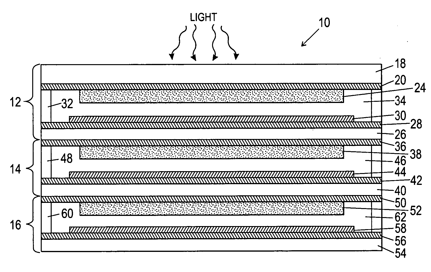
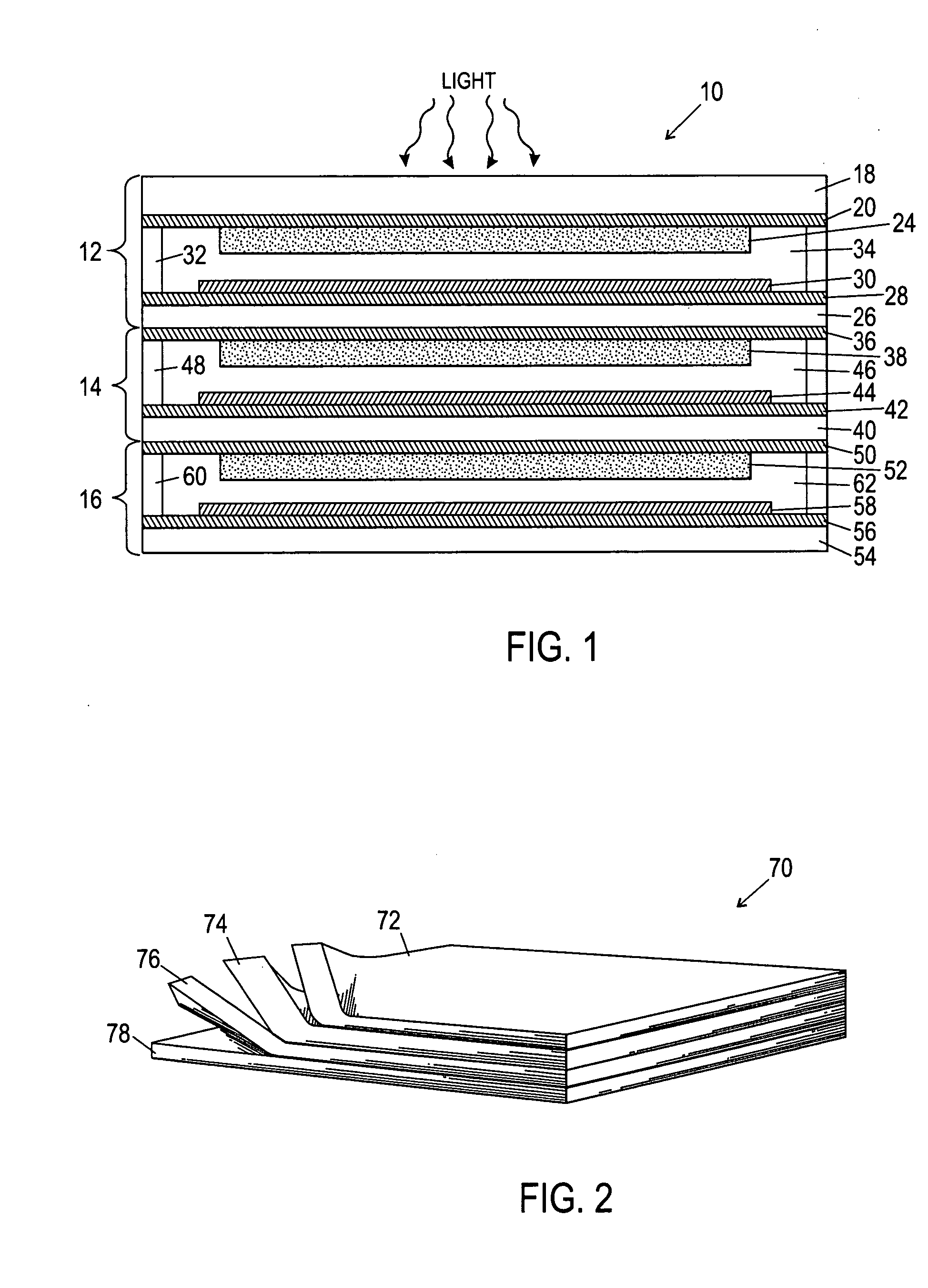
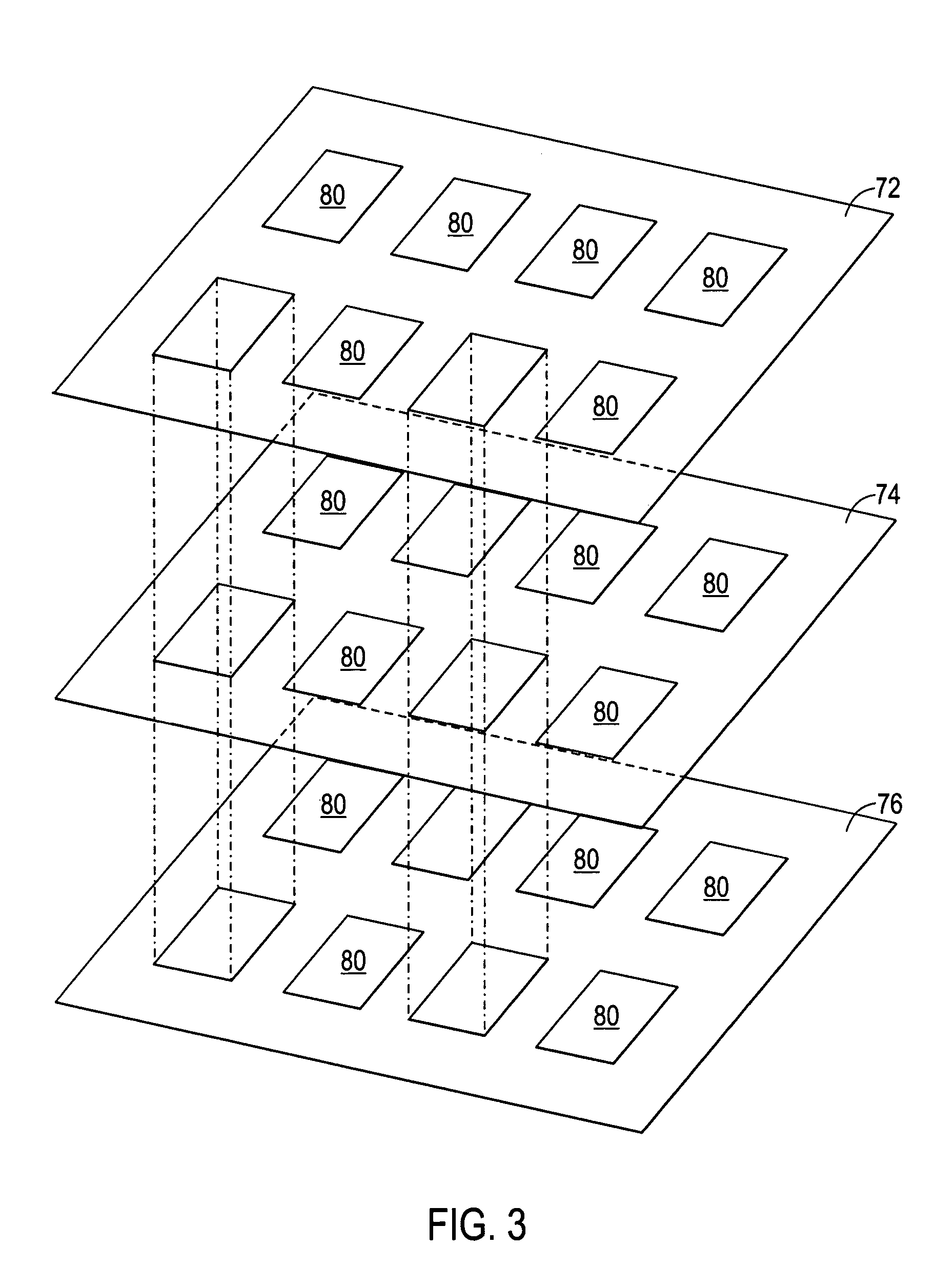
[0017] Organic electronic devices, such as photovoltaic (PV) devices, may be fabricated by depositing materials on substrates and laminating the substrates together to form a one or more solar cells stacked on top of each other. FIG. 1 illustrates a PV device 10 of the first embodiment of the present invention that comprises a plurality of PV modules 12, 14 and 16 arranged in a stack. Although the PV device 10 of FIG. 1 illustrates only three PV modules 12, 14 and 16, it should be understood that any desirable number of PV modules may be implemented in accordance with the present techniques. In addition, although FIG. 1 shows only one PV cell for each PV cell module, a PV cell module of the present invention can comprise a plurality of PV cells arranged in a grid pattern, as will be disclosed further below with reference to FIG. 3. Further, while the exemplary embodiment of FIG. 1 illustrates a dye sensitized PV cell, it should be understood that other types of PV cells may also be ...


PUM


Abstract

Interconnects for electronic devices. More specifically, stacked photoelectric devices, such as parallel tandem photovoltaic devices are provided. Each of the photovoltaic devices comprises photovoltaic cells formed between two substrates. Each of the substrates may include one or more interconnects to route a voltage from one side of the substrate to another. Each substrate includes an edge portion extending beyond the edge portion of an immediately adjacent substrate. All interconnects are exposed to one side of the device for easy and flexible electric connectivity and fabrication. The interconnects, which may include conductive vias or conductive edge wraps, are formed in the edge portion of the substrates.

Description

BACKGROUND OF THE INVENTION [0001] A photovoltaic (PV) cell is generally an electronic device that is capable of converting incident light into electricity (direct current). A photovoltaic cell comprises a pair of electrodes and light-absorbing and charge transporting photovoltaic materials disposed therebetween. When the photovoltaic material is irradiated with light, electrons that have been confined to an atom in the photovoltaic material are released by light energy to move freely. Thus, free electrons and holes are generated. The free electrons and holes are efficiently separated and transported to the electrodes through charge transporting materials so that electric energy is continuously extracted. Current commercial photovoltaic cells use a semiconductor photovoltaic material, typically silicon. However, implementing silicon for photovoltaic cells generally requires high product cost due to extensive material and energy consumption. Another type of commercial PV cell that ha...

Claims


Application Information

Patent Timeline
IPC IPC(8): H01L31/042
CPCH01G9/2031H01G9/2072H01G9/2095H01L31/043H01L31/042Y02E10/542H01L27/301H01L31/02008H01L31/0504Y02P70/50H10K39/10
Inventor GUI, JOHN YUPENGDELGADO, ELADIO CLEMENTE
Owner GENERAL ELECTRIC CO
Why Eureka
Try Eureka