

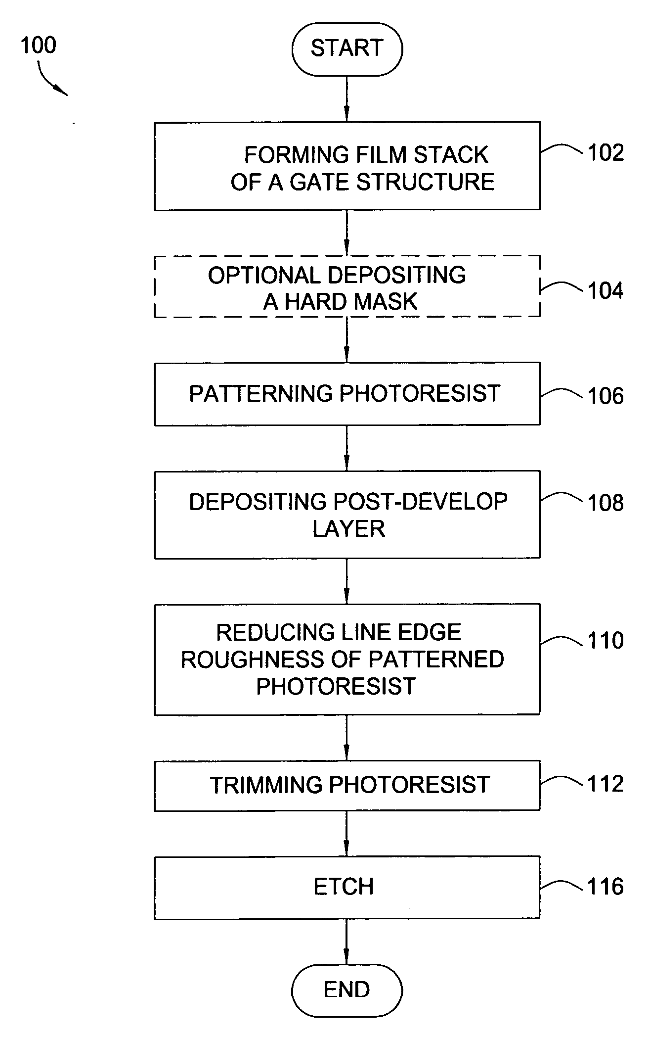
Line edge roughness reduction compatible with trimming
a technology of line edge roughness and trimming, which is applied in the direction of semiconductor devices, instruments, photomechanical treatment, etc., can solve the problems of difficult to accurately define the gate electrode width using conventional lithographic techniques, and achieve the effect of reducing line edge roughness
- Summary
- Abstract
- Description
- Claims
- Application Information
AI Technical Summary
Benefits of technology
Problems solved by technology
Method used
Image

Examples
example
[0040] In one exemplary process, bottom antireflective coating (BARC) is etched with 20 sccm HBr, 60 sccm CF4, and 45 sccm oxygen at 4 mTorr with a plasma power of 400 W and bias of 60 W. The etch time at 19 W DC is 35 seconds. The trim step is performed with the same properties as the BARC etch, except the bias is 30 W and the time is 20 seconds. In a following hardmask etch step, a mixture of gases including 30 sccm SF6, 35 sccm CH2F2, 45 sccm N2, and 200 sccm He is introduced into a chamber at 4 mTorr with a plasma power of 450 W and bias of 60 W at 11 W DC.
[0041] A soft landing is performed with 300 sccm HBr and 6.5 sccm O2 at a pressure of 6 mTorr. The plasma power is 400 W and the bias is 30 W with a DC of 11 W. An overetch step is performed with 300 sccm HBr, 20 sccm HeO2, and 200 sccm He at 70 mTorr. The plasma power for the overetch is 300 W, the bias is 30 W, and the DC is 19 W.
[0042] The invention may be practiced using other semiconductor wafer processing systems where...
PUM
 Abstract
Description
Claims
Application Information