Globally asynchronous communication architecture for system on chip

a communication architecture and chip technology, applied in the field of network on chip, can solve the problems of high latency, difficult to make particular, and difficult to precisely adapt the throughput carried by the communication bus from the chip to the application implemented,

Inactive Publication Date: 2006-09-21
COMMISSARIAT A LENERGIE ATOMIQUE ET AUX ENERGIES ALTERNATIVES
View PDF2 Cites 129 Cited by
  • Summary
  • Abstract
  • Description
  • Claims
  • Application Information

AI Technical Summary

Problems solved by technology

In particular, this system has the disadvantage of having low communication throughputs that could result in a high latency, and it is increasingly difficult to make particularly in terms of clock trees, particularly due to capacitive charge problems.
It is also difficult to precisely adapt the throughput carried by a communication bus from a chip to the application implemented by all modules on the chip.
Furthermore, such a system is usually very specific to a given application and generally cannot be reused in another application, once it has been designed for one application.
The use of such an architecture can be complex, particularly concerning placement-routing of its elements, and the production of its clock tree.
It is also difficult to control the consumption of such a network, particularly to control consumption due to the clock tree.
It is also difficult to control the consumption of such a network, particula

Method used


Image

  • Globally asynchronous communication architecture for system on chip
  • Globally asynchronous communication architecture for system on chip
  • Globally asynchronous communication architecture for system on chip

Examples


Embodiment Construction

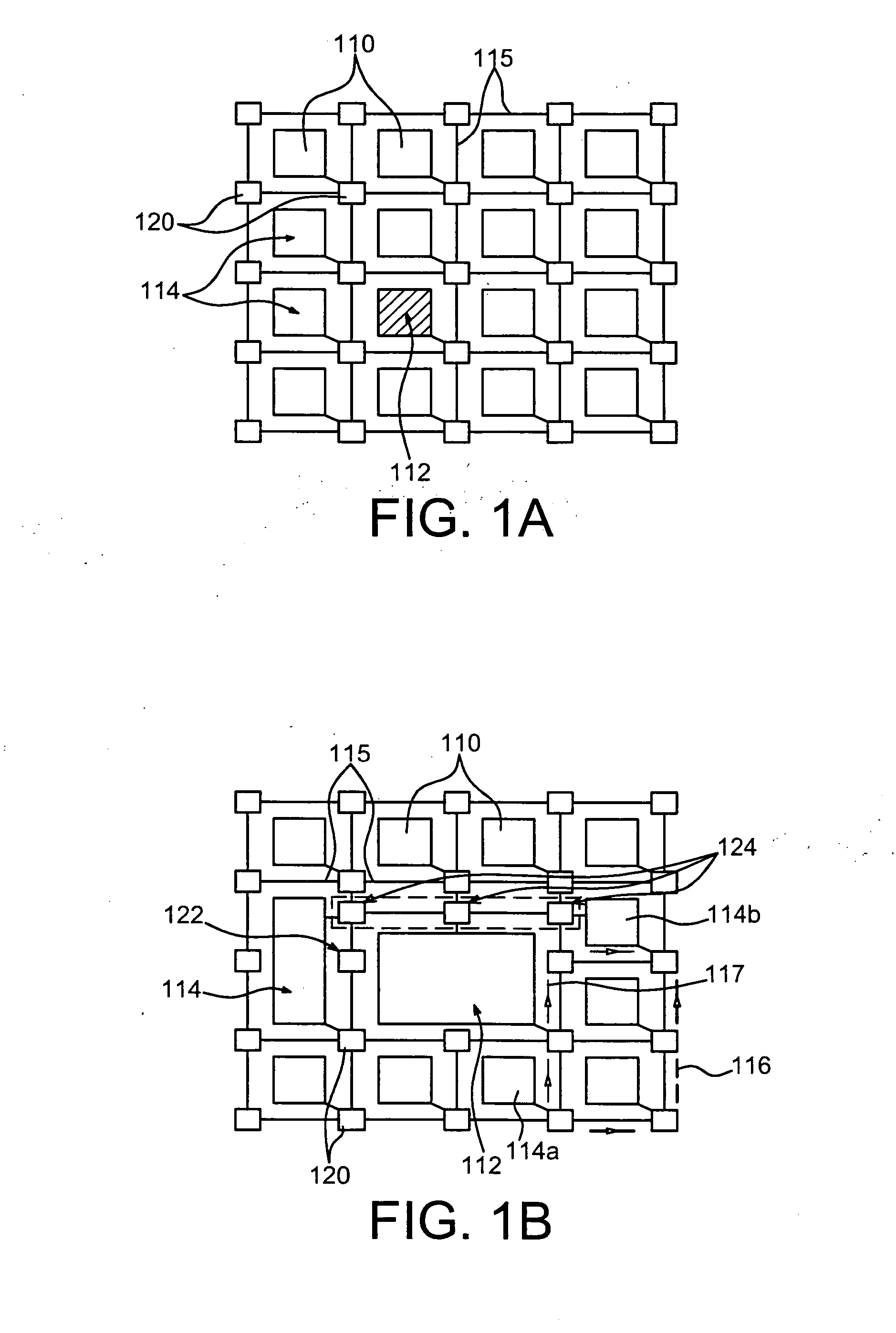
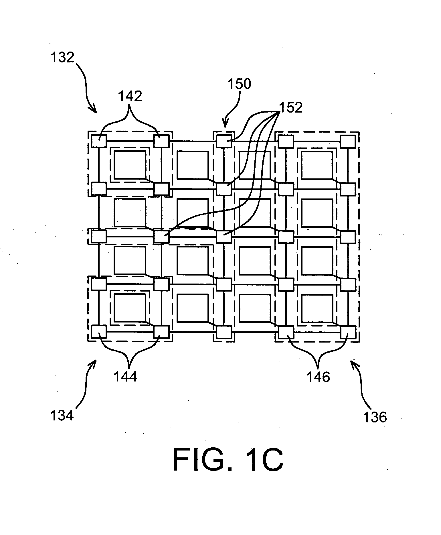
[0098]FIG. 1A shows an example of a communication or network on chip (NoC) architecture used according to the invention and provided with a matrix or “mesh” type topology.

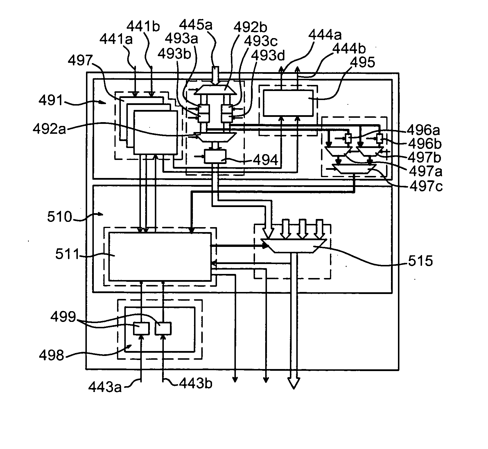
[0099] This architecture comprises a plurality of elements referenced 110 capable of processing data, and communicating with each other particularly by exchanging data. The set of elements 110 included in such an architecture may include an element denoted 112 acting as master and used particularly to initiate communications on the network. This element 112 that will be called the “network controller” can thus program communications between a plurality of other network elements that will be called “resources”114 and that can be used to perform tasks such as processing of elementary data, for example calculations, or for data storage or for encoding / decoding of data. The network controller 112 may for example be in the form of a processor or a micro controller. Some of the particular functions performed by the micr...


PUM


Abstract

This invention relates to the domain of Networks on Chips (NoC) and relates to a method of transferring data in a network on chip, particularly using an asynchronous “send/accept” type protocol. The invention also relates to a network on chip used to implement this method.

Description

TECHNICAL DOMAIN AND PRIOR ART [0001] This invention relates to the domain of Networks on Chips (NoC). It relates to a method of transferring data in a network on chip, particularly using an asynchronous “send / accept” type protocol and an improved network on chip structure, so that such transfers can be implemented. [0002] This structure can be made to operate globally asynchronously, even if it comprises units or blocks implemented in synchronous logic. This structure does not necessarily require a specialized logic, and it may comprise elements and particularly nodes implemented in synchronous logic, and other elements and particularly other nodes implemented in asynchronous logic. This structure is capable of performing different types of services, for example such as a “guaranteed latency” service and another service commonly called the “best effort” service. Implementation of these different services and management of priorities between data packets transiting in such a structu...

Claims


Application Information

Patent Timeline
IPC IPC(8): H04L12/56H04L12/28H04L12/54
CPCH04L12/56
Inventor CLERMIDY, FABIENVIVET, PASCALBEIGNE, EDITH
Owner COMMISSARIAT A LENERGIE ATOMIQUE ET AUX ENERGIES ALTERNATIVES
Why Eureka
Try Eureka