Process and photovoltaic device using an akali-containing layer

a photovoltaic device and akali-containing technology, applied in the direction of pv power plants, light radiation electric generators, generators/motors, etc., can solve the problems of low production capacity, relegated photovoltaics to niche markets, and difficult to produce pv cells on a commercial scale at the appropriate cost-basis critical for commercial viability

Inactive Publication Date: 2006-10-05
DAYSTAR TECHNOLOGIES
View PDF32 Cites 102 Cited by
  • Summary
  • Abstract
  • Description
  • Claims
  • Application Information

AI Technical Summary

Benefits of technology

[0023] When the mixed phase semiconductor source layer is formed, typically to a thickness of about 150 nm to about 500 nm, the alkali metals constitute between 5.0 to about 15.0 wt %. The alkali-containing mixed phase semiconductor source layer then incorporates with another p-type I-III-VI semiconductor layer, through the atomic exchange of sodium and other I-III-VI elements when thermally treated at high temperatures.

Problems solved by technology

However, to a large extent higher than desired product costs and lower than desired production capacities have relegated photovoltaics to niche markets only.
Even though relatively efficient PV cells can be manufactured in the laboratory, it has proven difficult to produce PV cells on a commercial scale at the appropriate cost-basis critical for commercial viability.
The coupling of the final alkali metal content in the CIGS absorber with the processing conditions during deposition is not conducive to a desired reproducibility and manufacturing control.
Until now, the incorporation of an alkali metal into CIGS absorbers has been difficult to achieve in actual practice, due to some particularities of the deposition process.
While the addition of sodium has been contemplated in other references, a practical method by which a sodium based alkali materials are added during the formation process has not yet been taught.
However, Stanbery does not disclose the principle of depositing alkali materials prior to deposition of a semiconductor layer with a subsequent thermal treatment.
However, Gillespie does not disclose a method for achieving this design, nor a process by which to form a sodium doped CIGS-type absorber.
However, Negami's process involves temperatures of up to 800° C. which would make manufacturing problematic and difficult.

Method used


Image

  • Process and photovoltaic device using an akali-containing layer
  • Process and photovoltaic device using an akali-containing layer
  • Process and photovoltaic device using an akali-containing layer

Examples


Embodiment Construction

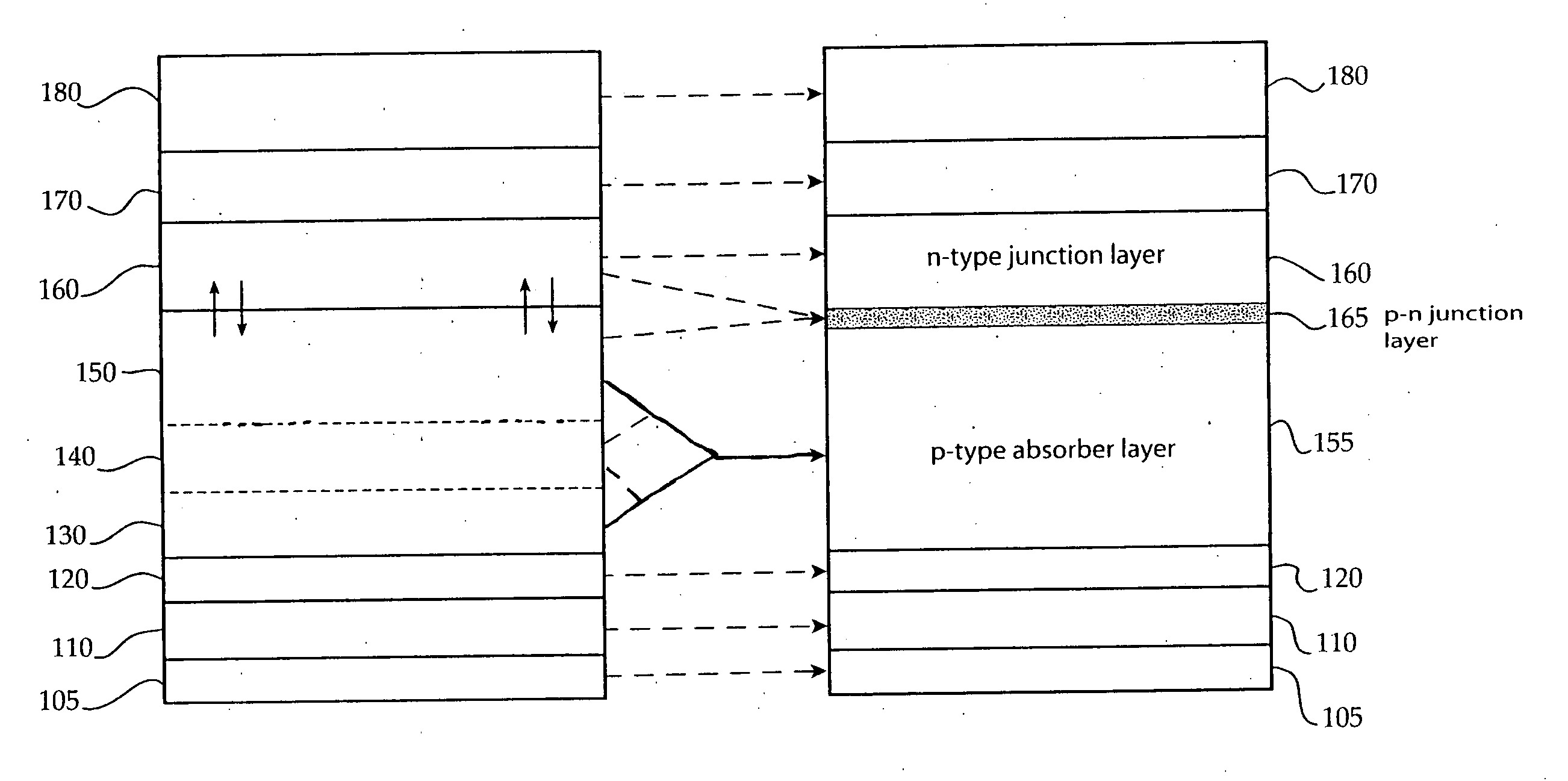
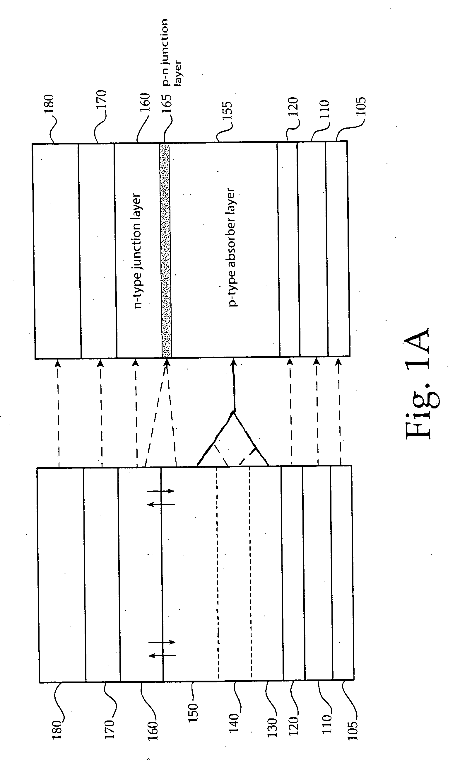
[0032] The present invention details an aspect in the production of photovoltaic (PV) devices with the aim of increasing energy efficiency and maximizing device production. More advanced PV technology has utilized alloys comprised of periodic table group I, III and VI elements for more advanced light energy absorption. Specifically, this invention enhances the quality of a Cu:In:Ga:Se p-type absorber (CIGS) in a photovoltaic device through the integration of alkali metals, such as sodium, and a semiconductor layer. Like many related embodiments, the PV cells in this embodiment are created through the sequential deposition of discrete layers. Methods of deposition may involve techniques such as sputtering, evaporation or other related deposition methods known to those skilled in the art.

[0033] Viewing FIG. 1A, all layers are deposited on a substrate 105 which may comprise one of a plurality of functional materials, for example, glass, metal, ceramic, or plastic. Deposited directly o...


PUM


Abstract

This invention describes the product and method of developing a photovoltaic device using an alkali-containing mixed phase semiconductor source layer to enhance cell efficiency and minimize molecular structure defects.

Description

CROSS-REFERENCE TO RELATED APPLICATIONS [0001] This application claims priority from U.S. Provisional Patent Application Ser. No. 60 / 626,843, filed Nov. 10, 2004.FIELD OF THE INVENTION [0002] This invention relates to the formation of thin-film photovoltaic device using an alkali-containing mixed phase semiconductor source layer. BACKGROUND OF THE INVENTION [0003] Alternative energy sources such as photovoltaic (PV) cells, modules, and power systems offer clean, reliable, renewable energy to the world's expanding demand for power. However, to a large extent higher than desired product costs and lower than desired production capacities have relegated photovoltaics to niche markets only. With the demand for energy going up, the world demand for alternatives to present energy sources is increasing. [0004] PV technologies offer a clean, non-carbon based alternative to traditional, non-renewable energy sources. The performance of a PV cell is measured in terms of its efficiency at conver...

Claims


Application Information

Patent Timeline
Patent Type & Authority Applications(United States)
IPC IPC(8): H02N6/00
CPCH01L31/0322Y02E10/541H01L31/0749
Inventor TUTTLE, JOHN R.
Owner DAYSTAR TECHNOLOGIES
Why Eureka
Try Eureka