Thin film transistor array panel for liquid crystal display

a thin film transistor and array panel technology, applied in the direction of optical elements, identification means, instruments, etc., can solve the problems of economic unsound cases, negative affecting the display characteristics of lcd, and several obstacles in reducing the aperture ratio of thin film transistors, so as to minimize misalignment problems and increase the aperture

Inactive Publication Date: 2006-10-19
SHENZHEN CHINA STAR OPTOELECTRONICS TECH CO LTD
View PDF24 Cites 32 Cited by
  • Summary
  • Abstract
  • Description
  • Claims
  • Application Information

AI Technical Summary

Benefits of technology

[0011] It is therefore an object of the present invention to provide a thin film transistor array panel for a liquid crystal display and methods for manufacturing the same, minimizing misalignment problems between two panels of an LCD and increasing its aperture.

Problems solved by technology

However, the misalignment of interlayes in fabricating a multi-layered structure negatively affects display characteristics of the LCD.
However, the LCD has several obstacles in reducing the aperture ratio of the thin film transistor.
Secondly, a black matrix must be wide enough to cover a possible misalignment of the two panels.
However, the latter case is economically unsound.
Because the color filters are formed after more expensive processes of forming thin film transistor, the failure in the color filter formation process wastes a lot of resources and increases the manufacturing costs.
On the other hand, the former method cannot generate enough storage capacitance between the gate line and the pixel electrode.

Method used


Image

  • Thin film transistor array panel for liquid crystal display
  • Thin film transistor array panel for liquid crystal display
  • Thin film transistor array panel for liquid crystal display

Examples


first embodiment

[0122] A manufacturing method of a thin film transistor array panel according to the present invention will now be described with reference to the FIGS. 5A to 11B and FIGS. 1 to 4.

[0123] At first, as shown in FIGS. 5A and 5B, a conductive layer is deposited and patterned by dry or wet etching through a photolithography process to form a black matrix 22 on a transparent insulating substrate 10.

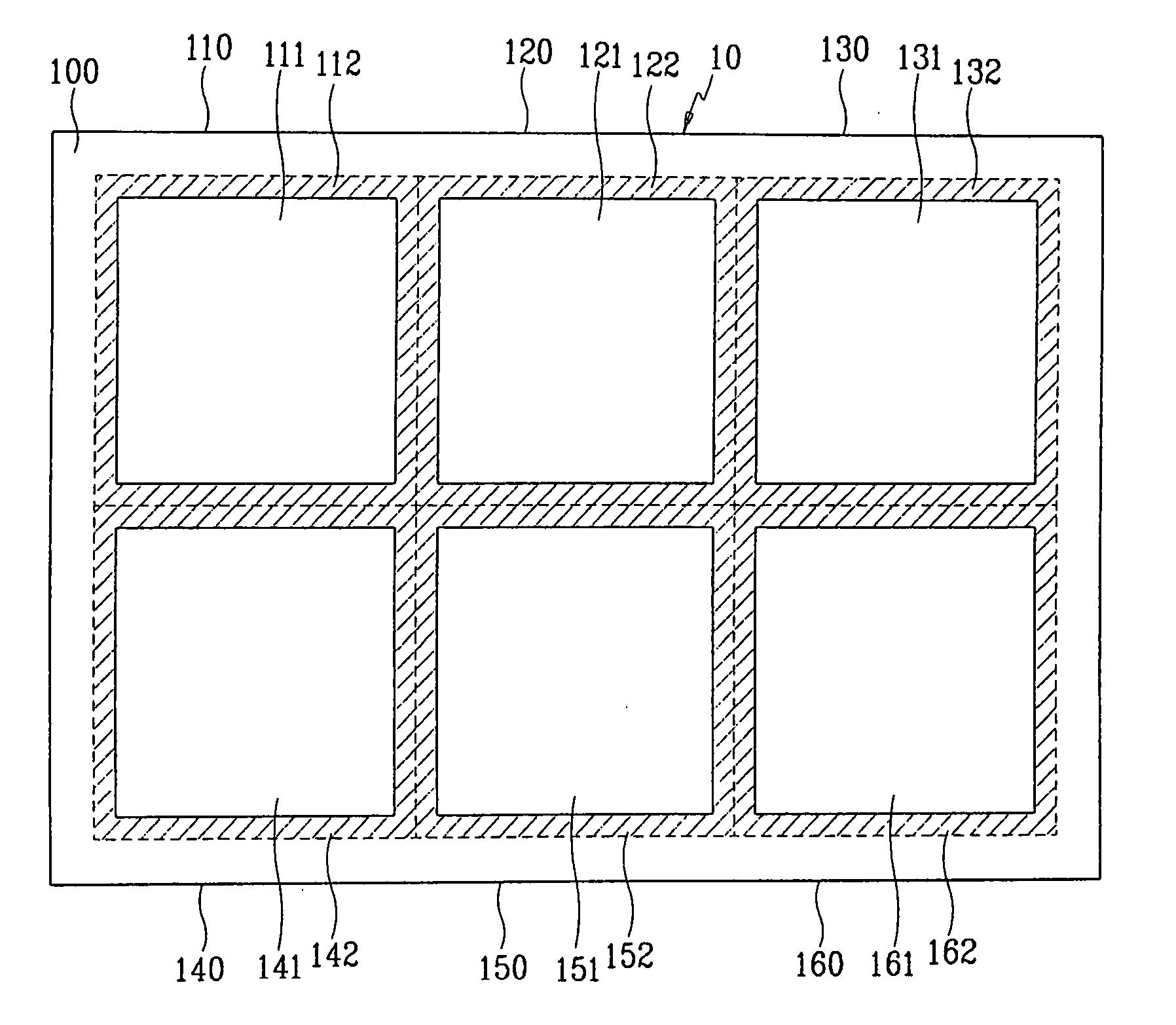
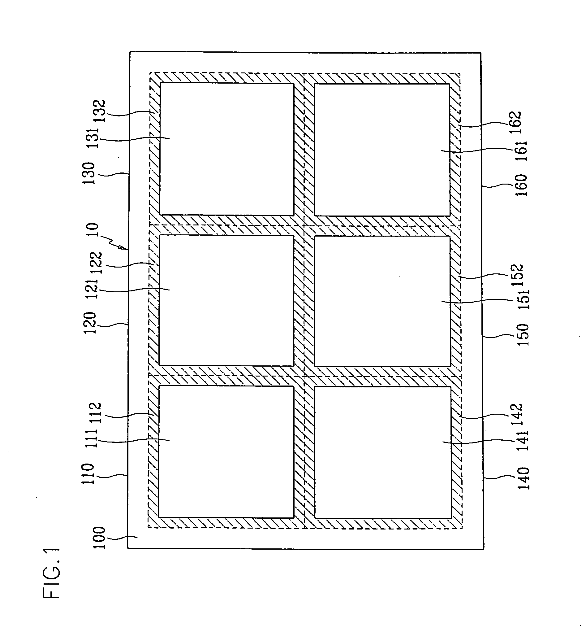
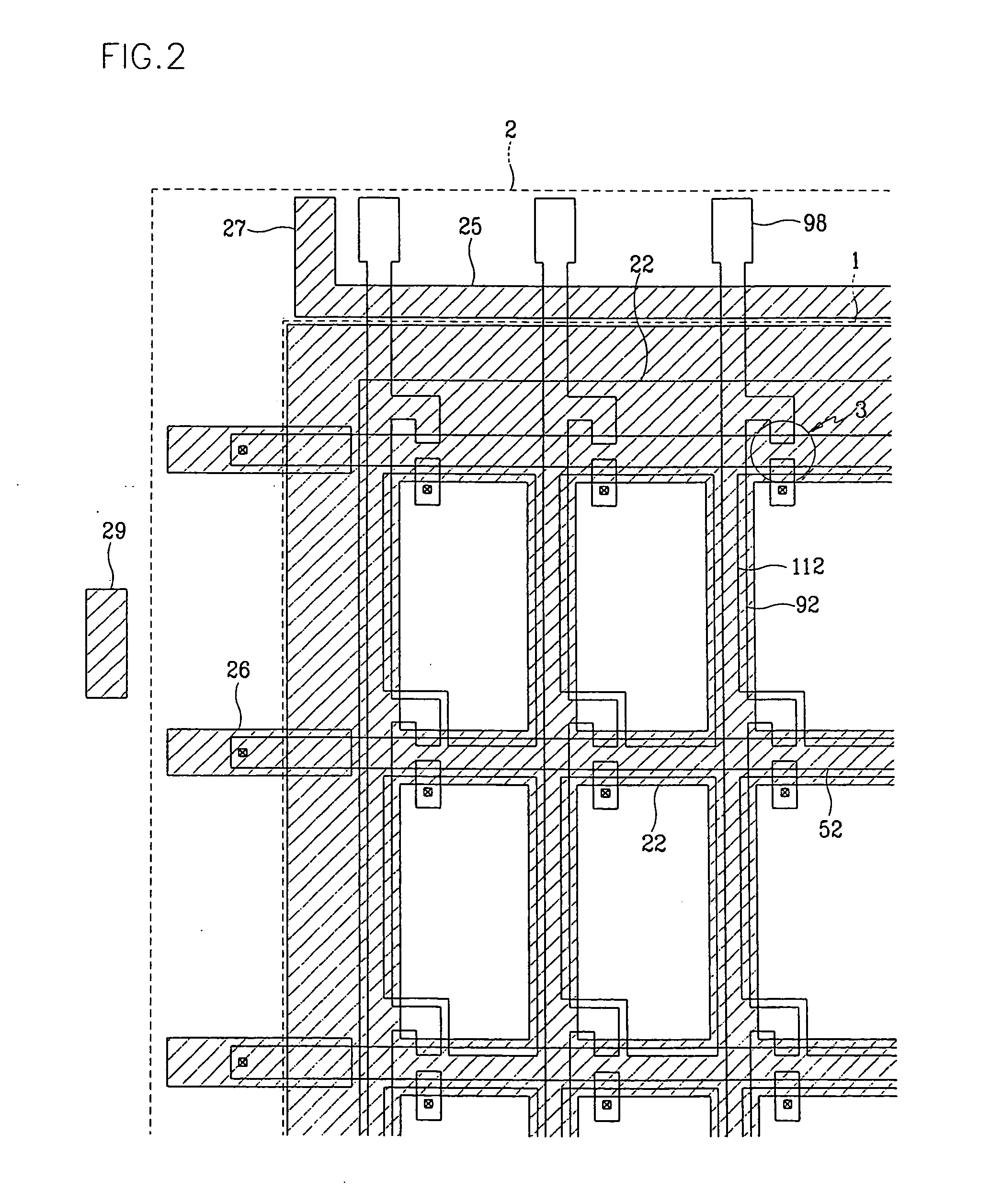
[0124] Here, a common wire including a common signal line 25 and a common pad 27, and a gate pad 26 may formed at the edge circumference of the peripheral areas 112, 122, 132, 142, 152 and 162 (referring to FIG. 1) of the substrate 10, and an alignment key 29 is formed at the outer area 100 (referring to FIG. 1).

[0125] If the alignment key 29 is formed when forming the black matrix 22, a plurality of thin films including a gate wire 52, 56 and a data wire 92, 95 and 96, which will be formed later, may be correctly aligned.

[0126] Here, the conductive material may include a material having a l...

third embodiment

[0186]FIG. 23 is a layout view of a TFT array panel for an LCD according to the present invention, and FIG. 24 is cross-sectional view taken along the line XXIV-XXIV′ of the FIG. 23. Here, a lower and an upper insulating substrates 101 and 201 are together shown in FIG. 24.

[0187] Data wires comprising a lower layer 901 including aluminum, aluminum alloy, copper or copper alloy, and an upper layer 902 of chromium, molybdenum, molybdenum alloy, chromium nitride or molybdenum nitride is formed on a lower insulating substrate 10. Data wire parts including a data line 92 extending in the vertical direction on FIG. 23, a data pad 98 connected to an end of data line 92 and transmitting image signals from an external circuit to the data line 92 and a light blocking layer 91 that blocks light reaching a semiconductor layer 70 of thin film transistor from the bottom of the substrate 10, and is connected to the data line 92. Here, the light blocking layer 91 may be used as a black matrix block...

fifth embodiment

[0244] As shown in FIGS. 34 and 35, most of the structure is similar to that of the third example.

[0245] However, a first redundant gate pad 94 including a lower layer 901 and an upper layer 902 is formed of the same layer as the data wire 91, 92 and 98, and an organic insulating layer has contact holes 41, 42, 44 and 48 respectively exposing a data line 92, the first redundant gate pad 94 and the data pad 98. Also, gate wires 52, 54 and 56 having a single-layered structure made of aluminum, aluminum alloy, copper or copper alloy is formed on the organic insulating layer 40. Here, the gate pad 54 is connected to the first redundant gate pad 94. A gate insulating layer 60 has contact holes 61, 64, 68 respectively exposing the data line 92, the first redundant gate pad 94 and the data pad 98, and a source ITO electrode 111 and a second redundant gate pad 114, which are respectively connected to the data line 92 and the first redundant gate pad 94 through 41 and 61, and 44 and 64, are...


PUM

PropertyMeasurementUnit
temperatureaaaaaaaaaa
dielectric constantaaaaaaaaaa
thicknessaaaaaaaaaa

Abstract

A black matrix having an opening at pixels of a matrix array in a display area, a common wire including common pads and common signal lines, and gate pads in a peripheral area, and an alignment key in outer area to align interlayer thin films are formed on an insulating substrate. Red, blue and green color filters the edge of which overlap the black matrix are formed at the pixels on the insulating substrate, and an organic insulating layer covering the black matrix and the color filters and having a contact hole exposing the gate pad is formed thereon. A gate wire including a gate line connected to the gate pad through the contact hole and a gate electrode connected to the gate line is formed on the organic insulating layer, and a gate insulating layer covering the gate wire is formed on the organic insulating layer. A semiconductor pattern and ohmic contact layers are sequentially formed on the gate insulating layer of the gate electrode. A data wire including a source electrode and a drain electrode that are made of a same layer on the ohmic contact layers and separated from each other, and a data line connected to the source electrode and defining the pixels of a matrix array by crossing the gate line is formed on the gate insulating layer. A passivation layer covering the data wire and having contact holes exposing the gate pad and the data pad is formed, and a pixel wire including a pixel electrode, a redundant gate pad, a redundant data pad that are respectively connected to the drain electrode, the gate pad and the data pad through the contact holes.

Description

CROSS-REFERENCE TO RELATED APPLICATIONS [0001] This application is a Continuation of U.S. patent application Ser. No. 10 / 660,779 filed Sep. 12, 2003, which is a Divisional of U.S. patent application Ser. No. 09 / 676,813 filed on Oct. 2, 2000, now U.S. Pat. No. 6,674,495, which claims priority to Korean Application No. 99-42180 filed on Sep. 30, 1999, Korean Patent Application No. 99-62915 filed on Dec. 27, 1999, Korean Patent Application No. 2000-52182 filed on Sep. 4, 2000, and Korean Patent Application No. 2000-52184, filed on Sep. 4, 2000, the entireties of which are incorporated herein by reference.BACKGROUND OF THE INVENTION [0002] (a) Field of the Invention [0003] The present invention relates to thin film transistor array panels for a liquid crystal display and the methods for manufacturing the same. [0004] (b) Description of the Related Art [0005] A liquid crystal display (LCD) is one of the most popular flat panel displays (FPDs). The liquid crystal display has two panels ha...

Claims


Application Information

Patent Timeline
Patent Type & Authority Applications(United States)
IPC IPC(8): H01L33/00G02B5/00G02B5/20G02F1/1335G02F1/136G02F1/1362G02F1/1368G09F9/30
CPCG02F1/136209G02F1/136227G02F1/136286G02F2001/136222H01L27/1255H01L29/42384H01L29/4908H01L27/1288H01L27/12G02F1/136222
Inventor HONG, MUN-PYOHONG, WAN-SHICKKIM, SANG-ILRHO, SOO-GUYKANG, JIN-KYUKIM, SNAG-GAB
Owner SHENZHEN CHINA STAR OPTOELECTRONICS TECH CO LTD
Why Eureka
Try Eureka