Apparatus and method for making circuitized substrates having photo-imageable dielectric layers in a continuous manner

Inactive Publication Date: 2006-10-26
I3 ELECTRONICS
View PDF26 Cites 13 Cited by
  • Summary
  • Abstract
  • Description
  • Claims
  • Application Information

AI Technical Summary

Benefits of technology

[0021] It is, therefore, a primary object of the present invention to enhance the circuitized substrate art by pro

Problems solved by technology

Such transfer is costly and time-consuming, especially when involving multi-layered products, the most common of boards sold today in

Method used


Image

  • Apparatus and method for making circuitized substrates having photo-imageable dielectric layers in a continuous manner
  • Apparatus and method for making circuitized substrates having photo-imageable dielectric layers in a continuous manner
  • Apparatus and method for making circuitized substrates having photo-imageable dielectric layers in a continuous manner

Examples


Embodiment Construction

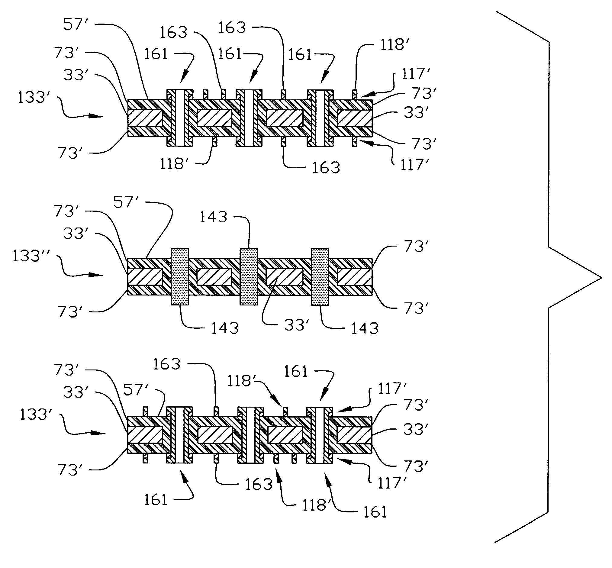
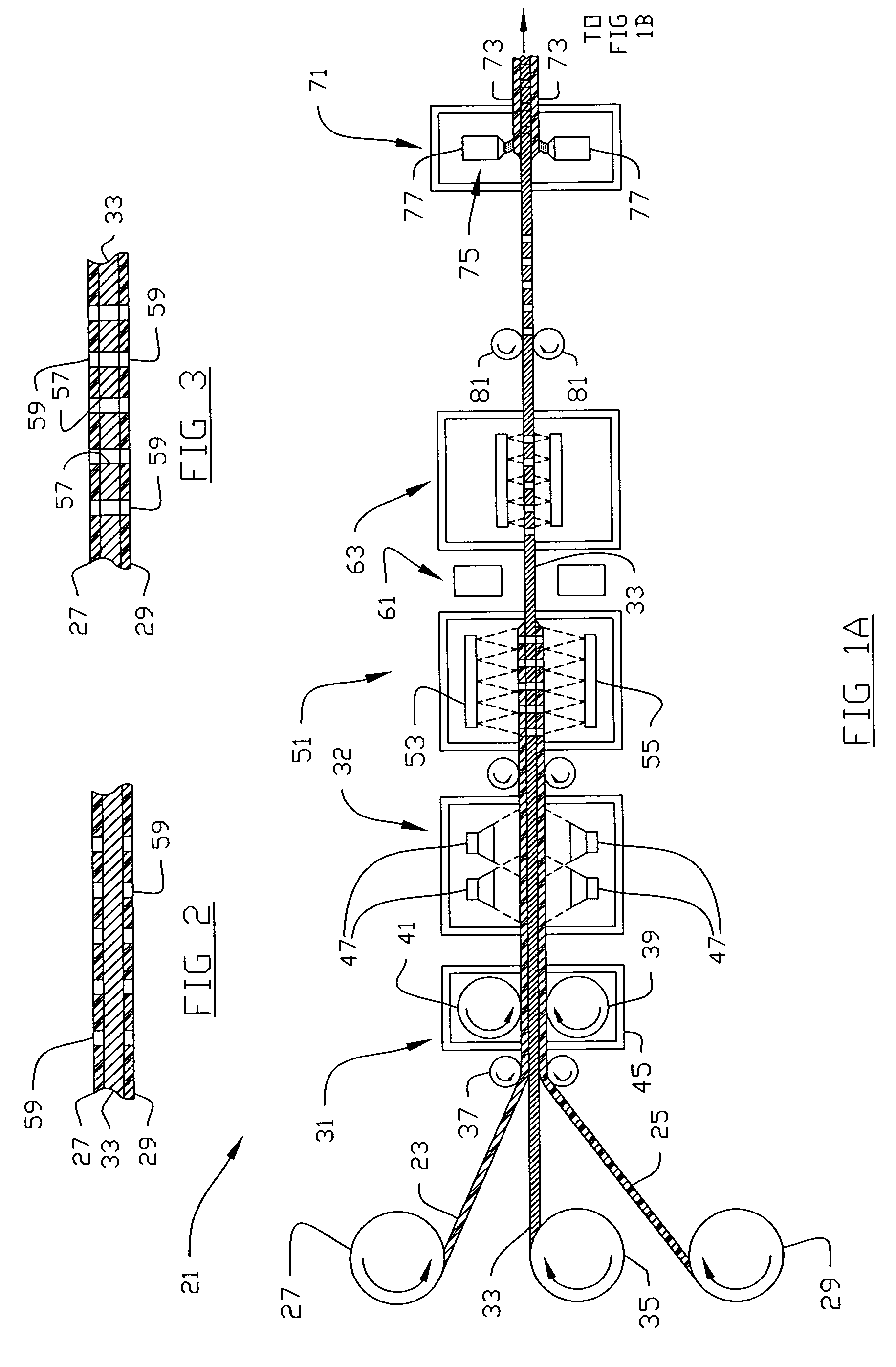
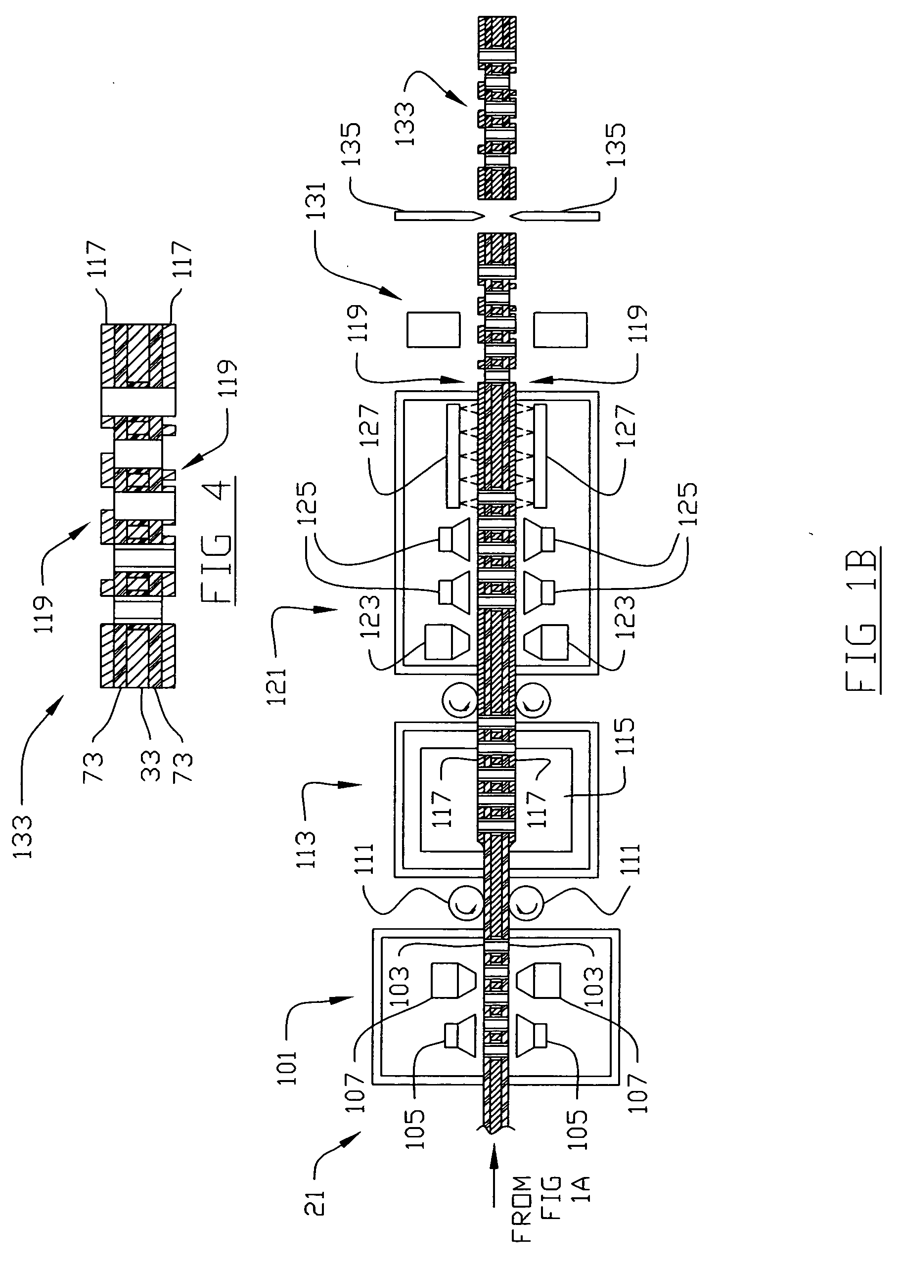
[0032] For a better understanding of the present invention, together with other and further objects, advantages and capabilities thereof, reference is made to the following disclosure and appended claims in connection with the above-described drawings. It is understood that like numerals will be used to indicate like elements from FIG. to FIG. By the term “continuous” as used herein when defining a process is meant a process in which all of the steps to manufacture a circuitized substrate having at least one conductive layer and two dielectric layers are performed with the at least one conductive layer being in the form of a continuous layer, up to final segmenting to define the final substrate's dimensions. All steps are performed while the conductive layer remains as provided from its original source (e.g., a roll), without segmenting occurring until the last step.

[0033] By the term “circuitized substrate” as used herein is meant to include substrates having at least two (and pre...


PUM

PropertyMeasurementUnit
Dielectric polarization enthalpyaaaaaaaaaa
Electrical conductivityaaaaaaaaaa
Electrical conductoraaaaaaaaaa

Abstract

Apparatus and method for making circuitized substrates using a continuous roll format in which a layer of conductor is fed into the apparatus, layers of photo-imageable dielectric are applied to opposite sides of the conductor layer, thru-holes are formed through the composite, and then metal layers are added over the dielectric and then patterns (e.g., circuit) are formed therein. Several operations are performed in addition to these to form the final end product, a circuitized substrate (e.g., printed circuit board), all while the conductor layer of the product is retained in a solid format, up to the final separation from the continuous layer.

Description

TECHNICAL FIELD [0001] This invention relates to the manufacture of circuitized substrates such as printed circuit boards, chip carriers, and the like. The invention particularly relates to the manufacture of such substrates in which conductive thru-holes are provided therein, and more particularly to those which utilize photo-imageable dielectric material for one or more of the substrate's dielectric layers. BACKGROUND OF THE INVENTION [0002] The conventional manufacture of circuitized substrates such as printed circuit boards and chip carriers, especially those of the multi-layered type, involves many individual processes such as etching, plating, lamination, drilling, testing, inspection, etc. Typically, these processes are performed at different locations within the manufacturing facility, requiring shipment of partially completed substrates from one station to another at such different locations. Such transfer is costly and time-consuming, especially when involving multi-layere...

Claims


Application Information

Patent Timeline
IPC IPC(8): G03F7/26
CPCH05K3/064Y10T29/49128H05K3/427H05K3/44H05K3/445H05K3/462H05K3/4641H05K2201/0355H05K2201/09536H05K2201/096H05K2201/10378H05K2203/0143H05K2203/068H05K2203/1545H05K2203/1572Y10T29/49165Y10T29/49155Y10T29/49126H05K3/4069
Inventor LAUFFER, JOHN M.MARKOVICH, VOYA R.MCNAMARA, JAMES J. JR.MOSCHAK, PETER A.
Owner I3 ELECTRONICS
Why Eureka
Try Eureka