Capacitor material for use in circuitized substrates, circuitized substrate utilizing same, method of making said circuitized substrate, and information handling system utilizing said circuitized substrate

Inactive Publication Date: 2006-07-13
TTM TECH NORTH AMERICA LLC
View PDF29 Cites 37 Cited by
  • Summary
  • Abstract
  • Description
  • Claims
  • Application Information

AI Technical Summary

Benefits of technology

[0029] It is, therefore, a primary object of the present invention to enhance the circuitized substrate art by providing a circuitized substrate havin

Problems solved by technology

The discrete passive devices occupy a high percentage of the surface area of the completed substrate, which is undesirable from a future design aspect because of the increased need and demand for miniaturization in today's substrates and products containing same art.
Some of the patents listed below, particularly U.S. Pat. No. 5,162,977, mention use of various materials for providing desired capacitance levels under this formula, and many mention or suggest problems associated with the methods and resulting materials used to do so.
Use of pre-fired and ground ceramic nano-powders in the dielectric layer poses obstacles for the formation of thru-holes (conductive holes permitting electronic communication between conductive layers of a PCB), however.
The distribution within the dielectric layer of particles of different size often presents major obstacles to thru-hole formation where the thru-holes are of extremely small diameter, also referred to in the industry as micro-vias due to the presence of the larger particles.
Another problem associated with pre-fired ceramic nano-powders is the ability for the dielectric layer to withstand substantial voltage without breakdown occurring across the layer.
This is even further undesirable because, as indicated by the equation cited above, greater planar capacitance may also be achieved by reducing the thickness of the dielectric layer.
That is, the re

Method used


Image

  • Capacitor material for use in circuitized substrates, circuitized substrate utilizing same, method of making said circuitized substrate, and information handling system utilizing said circuitized substrate
  • Capacitor material for use in circuitized substrates, circuitized substrate utilizing same, method of making said circuitized substrate, and information handling system utilizing said circuitized substrate
  • Capacitor material for use in circuitized substrates, circuitized substrate utilizing same, method of making said circuitized substrate, and information handling system utilizing said circuitized substrate

Examples


example one

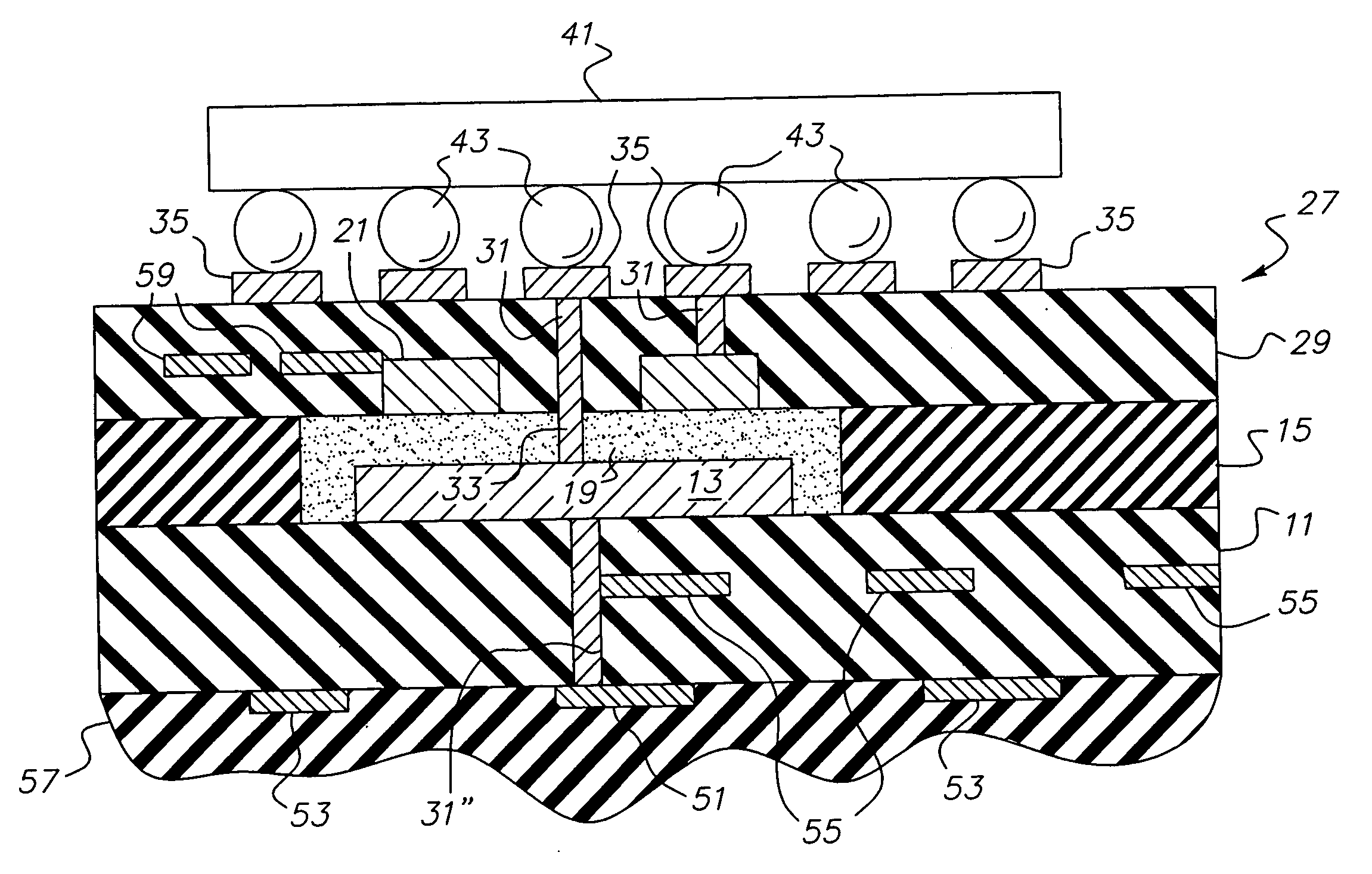
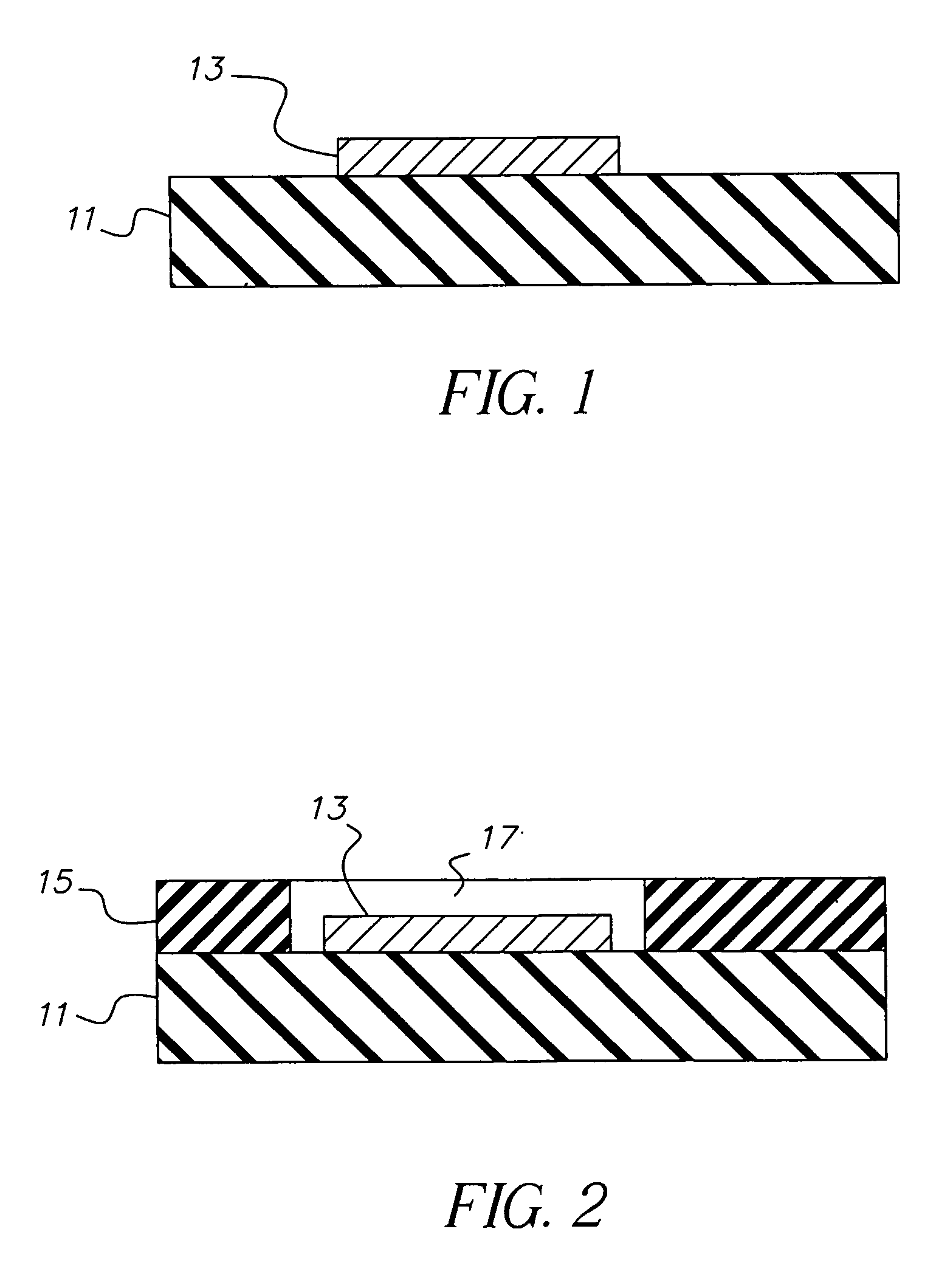
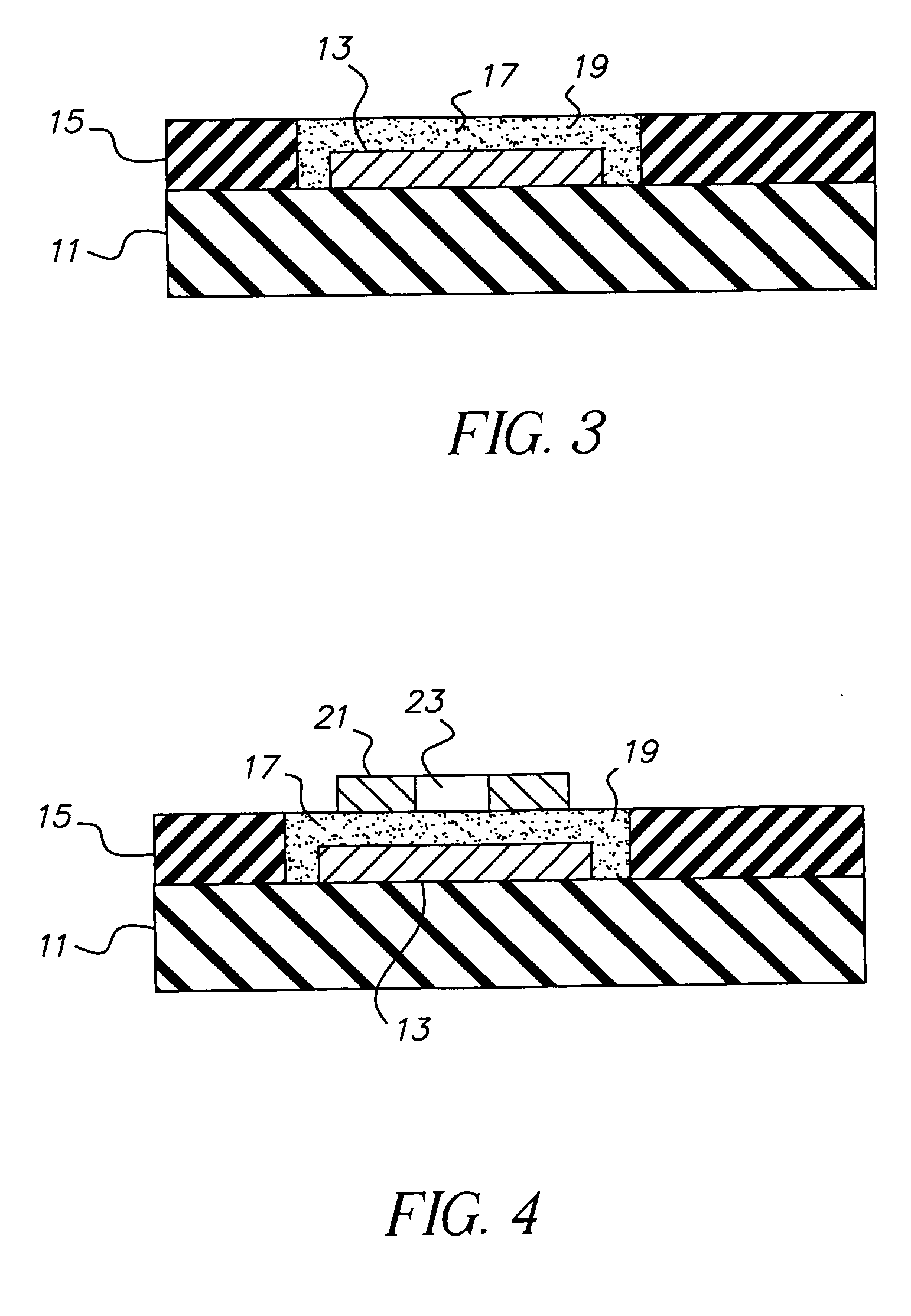
[0060] Fifty grams (gm) of cycloaliphatic epoxy resin (e.g., one sold under product designation “ERL-4211” by the Union Carbide Corporation, Danbury, Conn.) was mixed with about 50 gm of hexahydro-4-methylphthalic anhydride and 0.4 gm N,N dimethyl benzylamine. The mixed solution was stirred for 10 minutes to assure uniform mixing. Sixty gm of barium titanate (BaTiO3) powder available from the Nippon Chemical Industrial Co., Ltd., of Tokyo, Japan was added to 17.5 gm of the mixed solution and formed into a screen printable paste. A layer of this material was screened through a 145 mesh screen onto the top surface of a copper first electrical conductor. This layer was then cured at approximately 150° C. for about two hours. The second electrical conductor was then formed using a sputtering operation atop the cured screen printed material using a mask normally used for such sputtering operations. The resulting capacitance density of the formed capacitor measured about 5.5 nano-Farads(n...

example two

[0061] As in Example One, fifty grams (gm) of “ERL-4211” cycloaliphatic epoxy resin was mixed with about 50 gm of hexahydro-4-methylphthalic anhydride and 0.4 gm N,N dimethyl benzylamine. The mixed solution was stirred for 10 minutes to assure uniform mixing. 150 gm of a combination of barium titanate, calcium titanate and zirconium powders (also available from the Nippon Chemical Industrial Co., Ltd. Tokyo, Japan) was mixed thoroughly with 100 gm of the mixed solution and formed into a screen printable paste. A layer of this material was screened through a 200 mesh screen onto the top surface of a copper first electrical conductor. This layer was then cured at approximately 150° C. for about two hours, as in Example One. The second electrical conductor was then formed using a sputtering operation atop the cured screen printed material using a mask normally used for such sputtering operations. The average (mean) particle size for the added powder was about 0.2 micron, the surface ar...

example three

[0062] As in Examples One and Two, fifty grams (gm) of “ERL-4211” cycloaliphatic epoxy resin was mixed with about 50 gm of hexahydro-4-methylphthalic anhydride and 0.4 gm N,N dimethyl benzylamine. The mixed solution was stirred for 10 minutes to assure uniform mixing. 150 gm of Nippon Chemical Industrial's barium titanate powder was mixed thoroughly with 100 gm of the mixed solution and made into a screen printable paste. A layer of this paste material was screened through a 200 mesh screen onto the top surface of a copper first electrical conductor. This layer was then cured at approximately 150° C. for about two hours, as in Example One. The second electrical conductor was then formed using a sputtering operation atop the cured screen printed material using a mask normally used for such sputtering operations. The average (mean) particle size for the added powder was about 0.1 micron, the surface area about 15.08 square meters / gm, and the specific gravity about 5.52.


PUM


Abstract

A material for use as part of an internal capacitor within a circuitized substrate includes a polymer (e.g., a cycloaliphatic epoxy or phenoxy based) resin and a quantity of nano-powders of ferroelectric ceramic material (e.g., barium titanate) having a particle size substantially in the range of from about 0.01 microns to about 0.90 microns and a surface area for selected ones of said particles within the range of from about 2.0 to about 20 square meters per gram. A circuitized substrate adapted for using such a material and capacitor therein and a method of making such a substrate are also provided. An electrical assembly (substrate and at least one electrical component) and an information handling system (e.g., personal computer) are also provided.

Description

CROSS REFERENCE TO CO-PENDING APPLICATIONS [0001] In Ser. No. 10 / 900,385, entitled “Circuitized Substrate With Internal Organic Memory Device, Method Of Making Same, Electrical Assembly Utilizing Same, and Information Handling System Utilizing Same” and filed Jul. 28, 2004 (inventors: S. Desai et al), there is defined a circuitized substrate comprised of at least one layer of dielectric material having an electrically conductive pattern thereon. At least part of the pattern is used as the first layer of an organic memory device which further includes at least a second dielectric layer over the pattern and a second pattern aligned with respect to the lower part for achieving several points of contact to thus form the device. The substrate is preferably combined with other dielectric-circuit layered assemblies to form a multilayered substrate on which can be positioned discrete electronic components (e.g., a logic chip) coupled to the internal memory device to work in combination ther...

Claims


Application Information

Patent Timeline
IPC IPC(8): H01L23/02
CPCH01L23/49822H01L2224/16235H01L2224/73253H01L2924/01012H01L2924/0102H01L2924/01078H01L2924/15311H01L2924/16195H01L2924/3011H05K1/162H05K3/0023H05K2201/0187H05K2201/0209H05K2201/0257H05K2201/09509H05K2201/09718H01L2924/01019H01L2924/01087H01L2224/16H01L2924/00011H01L2924/00014H01L2224/0401
Inventor DAS, RABINDRA N.LAUFFER, JOHN M.PAPATHOMAS, KOSTAS I.POLIKS, MARK D.
Owner TTM TECH NORTH AMERICA LLC
Why Eureka
Try Eureka