MOS Transistor Gates with Doped Silicide and Methods for Making the Same

a technology of mos transistor gates and doped silicide, which is applied in the direction of transistors, semiconductor devices, electrical equipment, etc., can solve the problems of gate leakage current tunneling through, limited ability to form very thin oxide films with uniform thickness, and electrical and physical limitations on the extent to which siosub>2 /sub>gate dielectrics can be made thinner, etc., to facilitate elimination or simplification of channel engineering and high melting temperature

Inactive Publication Date: 2006-11-02
VISOKAY MARK +1
View PDF9 Cites 36 Cited by
  • Summary
  • Abstract
  • Description
  • Claims
  • Application Information

AI Technical Summary

Benefits of technology

[0014] The invention relates to semiconductor devices and fabrication methods, wherein transistor gate structures are created using doped metal silicide materials. A first metal silicide is formed above a gate dielectric and the silicide is doped with n-type impurities for NMOS gates or with p-type impurities for PMOS gates. The inventors have appreciated that the gate work function of the resulting NMOS and PMOS transistors can be successfully adjusted through appropriate doping the gate silicide, thereby facilitating elimination or simplification of channel engineering. The doped first metal silicide may comprise a refractory metal such as molybdenum, tungsten, tantalum, titanium, or others having a high melting temperature, and may be formed by direct silicide deposition or through reacting metal and silicon deposited above the gate dielectric. In this regard, a single starting material may be employed to form both PMOS and NMOS gate structures, thus avoiding process integration problems associated with using different gate materials. Dopants may be added to the first silicide through any means, such as direct implantation into a reacted or deposited silicide or implantation into unreacted metal and / or unreacted silicon followed by annealing to concurrently diffuse the dopants into the metal and to create the resulting metal silicide, where the dopants can be introduced before or after gate patterning.

Problems solved by technology

However, there are electrical and physical limitations on the extent to which SiO2 gate dielectrics can be made thinner.
These include gate leakage currents tunneling through the thin gate oxide, limitations on the ability to form very thin oxide films with uniform thickness, and the inability of very thin SiO2 gate dielectric layers to prevent dopant diffusion from the gate poly-silicon into the underlying channel.
The depleted portion of the gate contact and the gate dielectric operate as series connected capacitors, resulting in a reduced effective gate capacitance, which reduces the drive current capability of the device.
Consequently, poly-silicon depletion causes reduction in device performance which leads to poor unscalable devices.
Simply increasing the implant energy and / or anneal time to combat poly-silicon depletion has adverse results, in that the corresponding depths of the concurrently implanted source / drain regions are increased.
However, as gate dielectrics and gate contacts continue to become smaller through scaling, the poly-silicon depletion problem is more pronounced, wherein poly-silicon depletion regions of 2 to 4 angstroms become a significant fraction of the overall effective gate capacitance.
Thus, while poly-silicon gate contacts have previously offered flexibility in providing dual work functions for CMOS processes, the future viability of conventional poly-silicon gate technology is lessened as scaling efforts continue.

Method used


Image

  • MOS Transistor Gates with Doped Silicide and Methods for Making the Same
  • MOS Transistor Gates with Doped Silicide and Methods for Making the Same
  • MOS Transistor Gates with Doped Silicide and Methods for Making the Same

Examples


Embodiment Construction

[0028] One or more implementations of the present invention will now be described with reference to the attached drawings, wherein like reference numerals are used to refer to like elements throughout, and wherein the illustrated structures are not necessarily drawn to scale. The invention relates to semiconductor devices, as well as MOS transistor gate structures and fabrication methods therefor, in which first and second metal silicides are formed in a gate structure and the first metal silicide is doped.

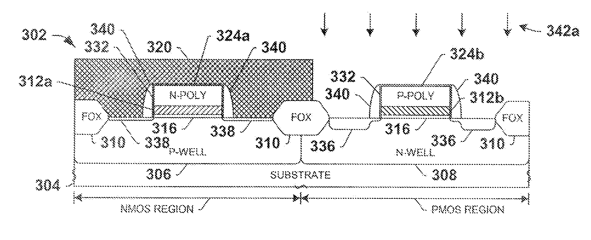
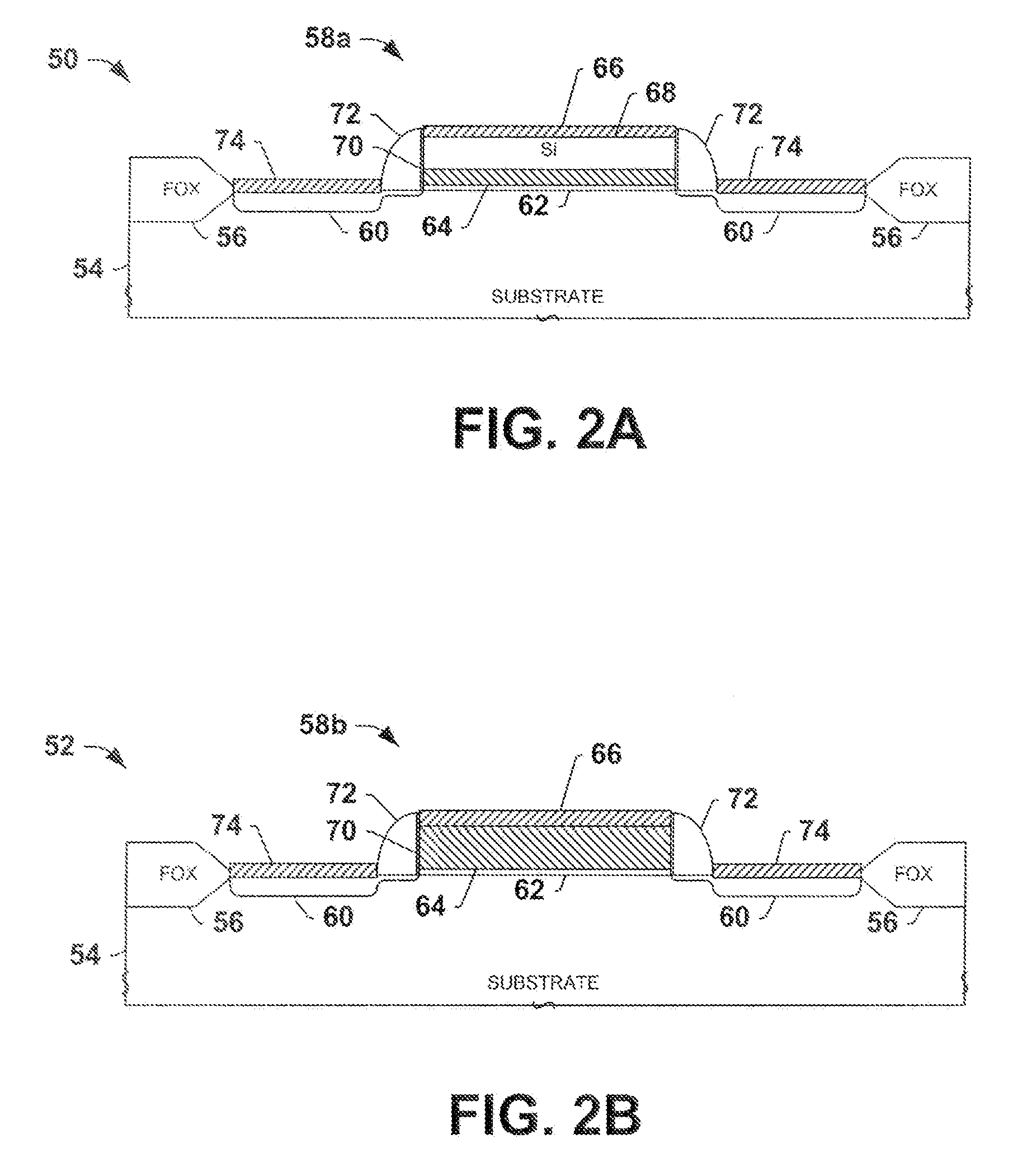
[0029]FIGS. 2A and 2B illustrate exemplary CMOS semiconductor devices 50 and 52, with NMOS transistors 58a and 58b, respectively, having gate structures in accordance with the invention. The devices 50, 52 are fabricated in or on a silicon substrate 54, although the invention may be carried out in association with SOI wafers, epitaxial silicon layers formed over silicon wafers, and any other semiconductor body. N-wells, p-wells, and / or buried layers (not shown) may be formed in t...


PUM

PropertyMeasurementUnit
electric fieldaaaaaaaaaa
threshold voltageaaaaaaaaaa
gate voltageaaaaaaaaaa

Abstract

Semiconductor devices and fabrication methods are presented, in which transistor gate structures are created using doped metal silicide materials. Upper and lower metal silicides are formed above a gate dielectric, wherein the lower metal silicide is doped with n-type impurities for NMOS gates and with p-type impurities for PMOS gates, and wherein a silicon may, but need not be formed between the upper and lower metal silicides. The lower metal silicide can be deposited directly, or may be formed through reaction of deposited metal and poly-silicon, and the lower silicide can be doped by diffusion or implantation, before or after gate patterning.

Description

FIELD OF INVENTION [0001] The present invention relates generally to semiconductor devices and more particularly to doped silicide MOS transistor gates and fabrication methods for making the same. BACKGROUND OF THE INVENTION [0002] Field effect transistors (FETs) are widely used in the electronics industry for switching, amplification, filtering, and other tasks related to both analog and digital electrical signals. Most common among these are metal-oxide-semiconductor field-effect transistors (MOSFETs), wherein a gate contact or electrode is energized to create an electric field in a channel region of a semiconductor body, by which electrons are allowed to travel through the channel between a source region and a drain region of the semiconductor body. The source and drain regions are typically formed by adding dopants to targeted regions on either side of the channel. A gate dielectric or gate oxide is formed over the channel, and a gate electrode or gate contact is formed over the...

Claims


Application Information

Patent Timeline
Patent Type & Authority Applications(United States)
IPC IPC(8): H01L29/788H01L21/8238
CPCH01L21/823842H01L21/823835
Inventor VISOKAY, MARKCOLOMBO, LUIGI
Owner VISOKAY MARK
Why Eureka
Try Eureka