Optical scanner having multi-layered comb electrodes

a comb electrode and optical scanner technology, applied in the field of microelectromechanical system optical scanners, can solve the problems of increasing the screen size of the display device, and the limitation of increasing the driving speed and the driving angle of the actuator, and achieve the effect of increasing the electrostatic for

Inactive Publication Date: 2006-11-30
SAMSUNG ELECTRONICS CO LTD
View PDF2 Cites 45 Cited by
  • Summary
  • Abstract
  • Description
  • Claims
  • Application Information

AI Technical Summary

Benefits of technology

[0022] According to still another aspect of the present invention, there is provided a method of driving a mirror stage of an optical scanner comprising at least one multi-layered driving comb electrode and at least one multi-layered fixed comb electrode, the method comprising: applying a predetermined voltage to each layer of the driving comb electrode and the fixed comb electrode; and changing the predetermined voltage applied to at least one layer of the driving comb electrode and the fixed comb electrode to increase an electrostatic force between the driving comb electrode and the fixed comb electrode.

Problems solved by technology

Also, as the driving angle of the optical scanner increases, the screen size of the display device increases.
However, since the driving speed and the driving angle of the actuator are in a trade-off relation, there is a limitation in increasing both the driving speed and the driving angle of the actuator.

Method used


Image

  • Optical scanner having multi-layered comb electrodes
  • Optical scanner having multi-layered comb electrodes
  • Optical scanner having multi-layered comb electrodes

Examples


Embodiment Construction

[0040] The present invention will now be described more fully with reference to the accompanying drawings, in which exemplary embodiments of the invention are shown. In the following description of the present invention, the sizes of constituent elements shown in the drawings may be exaggerated, if needed, or sometimes the elements may be omitted for a better understanding of the present invention. However, such ways of description does not limit the scope of the technical concept of the present invention.

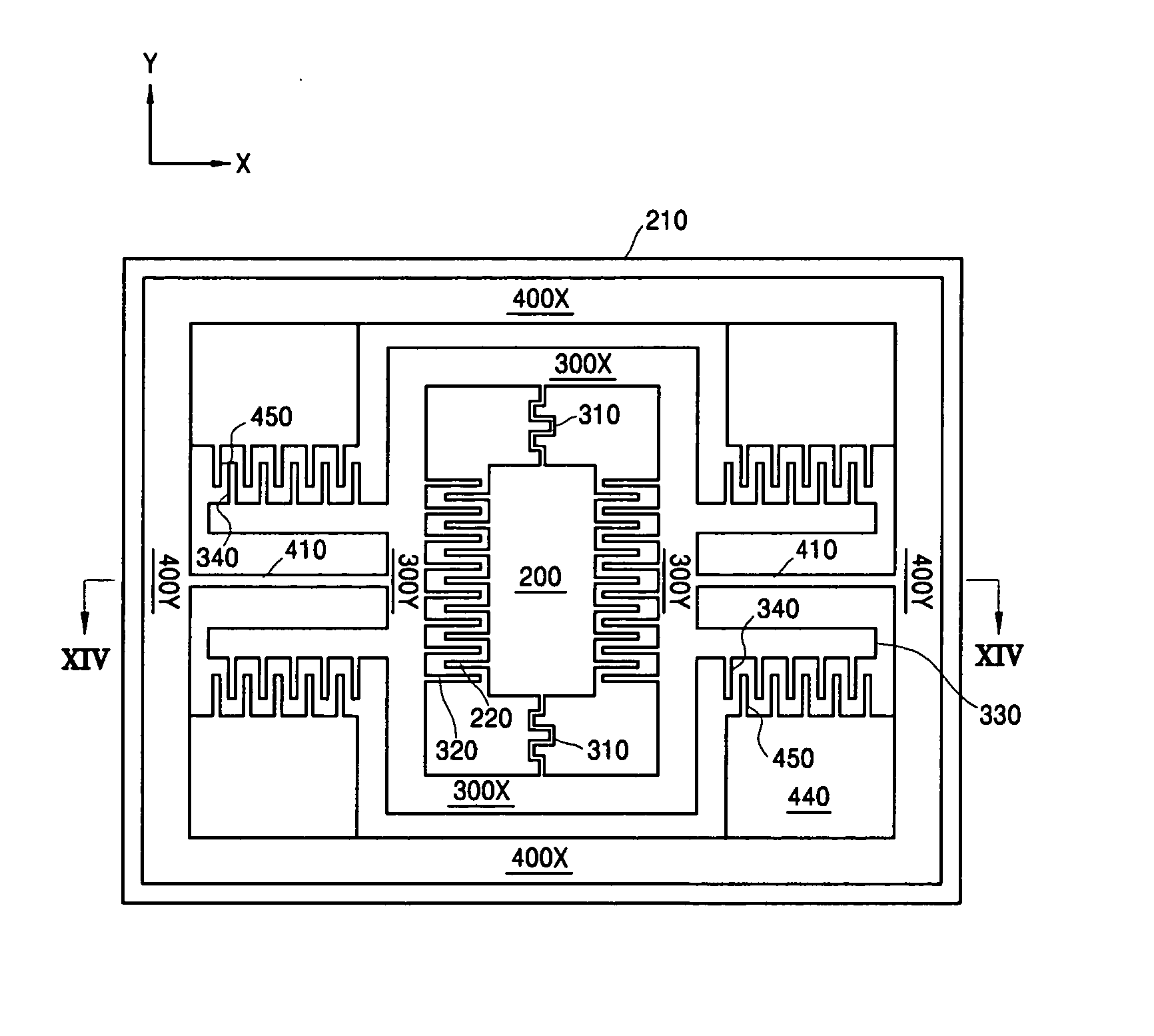
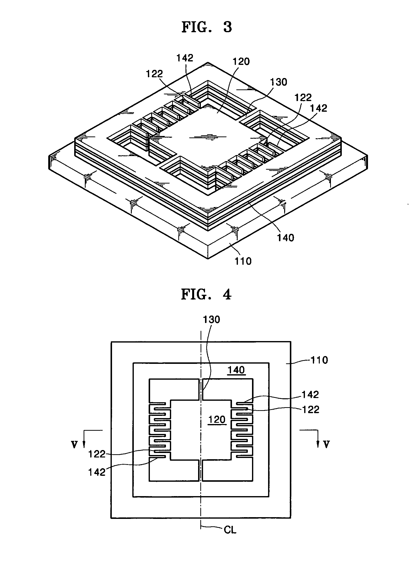
[0041]FIG. 3 is a perspective view of an optical scanner according to an exemplary embodiment of the present invention. FIG. 4 is a plan view of the optical scanner of FIG. 3. FIG. 5 is a cross-sectional view taken along line V-V of FIG. 4.

[0042] Referring to FIGS. 3 through 5, a stage 120 is suspended above a substrate 110 made of pyrex glass by a support unit that supports both sides of the stage 120. The support unit includes torsion springs 130, which are connected to middle ...


PUM


Abstract

Optical scanners having a multi-layered comb electrode structure and methods to increase driving force and angle are provided. The optical scanner includes: a stage which performs a seesaw motion in a first direction; a support unit which supports the seesaw motion of the stage; and a stage driving unit including driving comb electrodes extending outward from opposite sides of the stage in the first direction and fixed comb electrodes extending from the support unit facing the driving comb electrodes such that the driving comb electrodes and the fixed comb electrodes alternate with each other. Each of the stage, the support unit, and the stage driving unit is made of a plurality of conductive layers and insulation layers between the conductive layers.

Description

CROSS-REFERENCE TO RELATED PATENT APPLICATION [0001] This application claims priority, under 35 U.S.C. § 119, from Korean Patent Application No. 10-2005-0046128, filed on May 31, 2005, in the Korean Intellectual Property Office, the disclosure of which is incorporated herein in its entirety by reference. BACKGROUND OF THE INVENTION [0002] 1. Field of the Invention [0003] Apparatuses and methods consistent with the present invention relate to a micro-electro-mechanical system (MEMS) optical scanner, and more particularly, to an optical scanner having multi-layered comb electrodes formed on the same plane. [0004] 2. Description of the Related Art [0005] Optical scanners can be used for large display devices to scan a laser beam. In optical scanners, the driving speed of an actuator relates to the resolution of a display device, and the driving angle of the optical scanner relates to the screen size of the display device. That is, as the driving speed of the optical scanner increases, ...

Claims


Application Information

Patent Timeline
Patent Type & Authority Applications(United States)
IPC IPC(8): G02B26/08G02B26/00H02N1/00
CPCH02N1/008G02B26/0841
Inventor CHO, JIN-WOOKO, YOUNG-CHULLEE, JIN-HOJEONG, HYUN-KU
Owner SAMSUNG ELECTRONICS CO LTD
Why Eureka
Try Eureka