Rewriteable memory cell comprising a transistor and resistance-switching material in series

a memory cell and transistor technology, applied in the direction of bulk negative resistance effect devices, semiconductor devices, electrical devices, etc., can solve the problems of difficult to form a large, high-density array of such cells, provide precisely controlled read, and s

Inactive Publication Date: 2006-12-07
SANDISK TECH LLC
View PDF46 Cites 229 Cited by
  • Summary
  • Abstract
  • Description
  • Claims
  • Application Information

AI Technical Summary

Benefits of technology

[0004] The present invention is defined by the following claims, and nothing in this section should be taken as a limitation on those claims. In general, the invention is directed to a nonvo...

Problems solved by technology

It is very difficult to form a large, high-density array of such cells, however, due to the danger of disturbance between cells, high...

Method used


Image

  • Rewriteable memory cell comprising a transistor and resistance-switching material in series
  • Rewriteable memory cell comprising a transistor and resistance-switching material in series
  • Rewriteable memory cell comprising a transistor and resistance-switching material in series

Examples


first embodiment

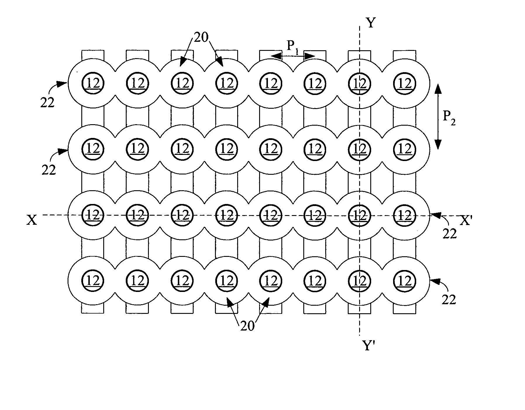
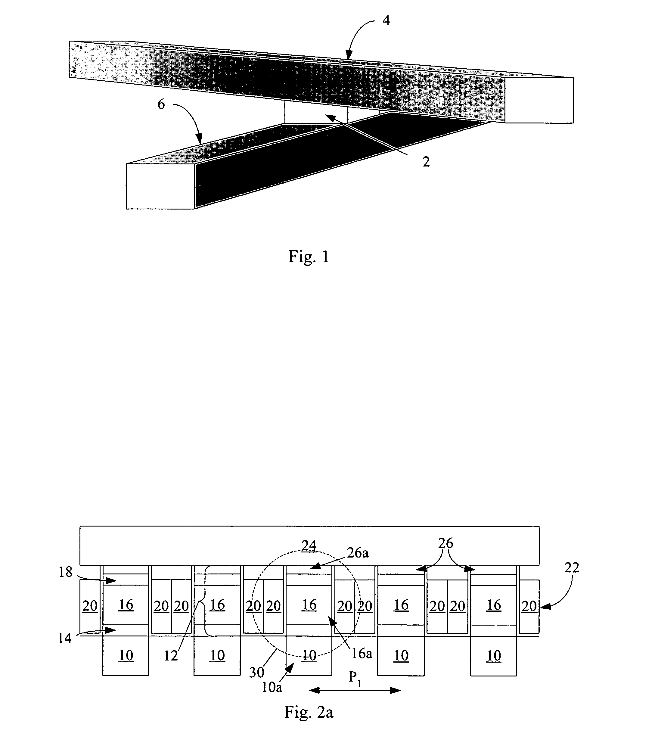
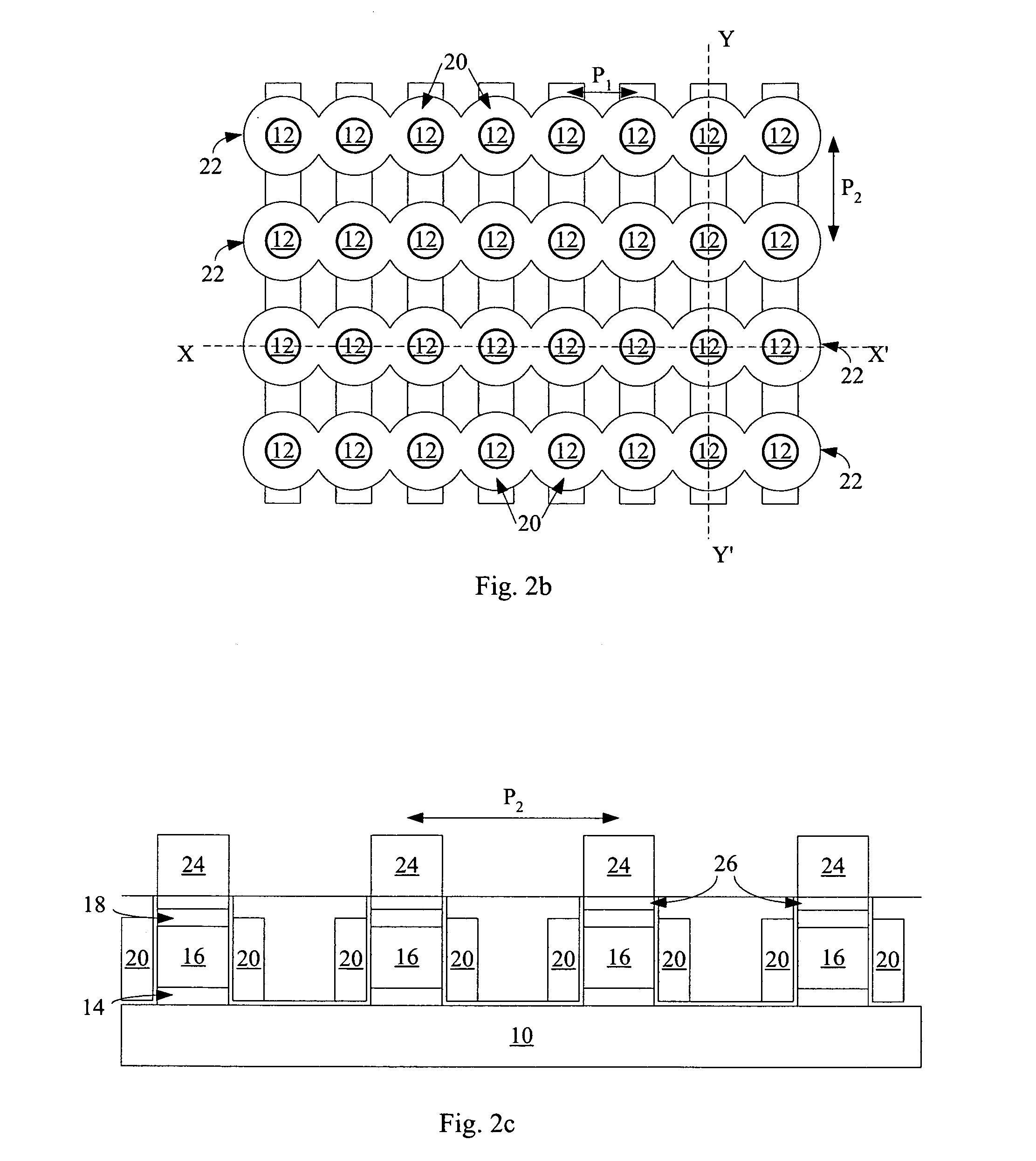
[0016]FIGS. 4a-4j are views showing stages in formation of the present invention. FIGS. 4c and 4j are plan views; the rest are cross-sectional views.

[0017]FIG. 5 is a cross-sectional view showing two memory levels according to the embodiment of FIGS. 4a-4j sharing reference lines.

[0018]FIG. 6a is a cross-sectional view showing four memory levels according to the embodiment of FIGS. 4a-4j sharing reference lines and data lines. FIG. 6b is a cross-sectional view showing four memory levels according to the embodiment of FIGS. 4a-4j sharing reference lines, but not sharing data lines.

[0019]FIGS. 7a-7c are circuit diagrams describing voltages applied to set, reset, and read a selected memory cell S in an array formed according to the first embodiment of the present invention.

second embodiment

[0020]FIGS. 8a-8g are cross-sectional views showing stages in formation of the present invention.

[0021]FIGS. 9a-9c are circuit diagrams describing voltages applied to set, reset, and read a selected memory cell S in an array formed according to the second embodiment of the present invention.


PUM


Abstract

A nonvolatile memory cell is provided, the cell comprising a transistor in series with resistance-switching material, which can be switched between at least two stable resistance states, for example a high-resistance state and a low-resistance state. In preferred embodiments the transistor is a TFT, having a channel region not formed in a monocrystalline wafer substrate. In preferred embodiments the transistor may have either a vertically oriented channel or a laterally oriented channel. Either embodiment can be formed in a monolithic three dimensional memory array in which multiple memory levels can be formed above a single substrate, forming a highly dense nonvolatile memory array.

Description

BACKGROUND OF THE INVENTION [0001] The invention relates to a nonvolatile memory cell comprising a reversible resistance-switching memory element. [0002] Resistance-switching materials, which can reversibly be converted between a high-resistance state and a low-resistance state, are known. These two stable resistance states make such materials an attractive option for use in a rewriteable non-volatile memory array. It is very difficult to form a large, high-density array of such cells, however, due to the danger of disturbance between cells, high leakage currents, and the difficulty of providing precisely controlled read, set, and reset voltages to the resistance-switching material. [0003] There is a need, therefore, for a nonvolatile memory cell having a reversible resistance-switching memory element which can readily be adapted for use in a large, highly dense monolithic three dimensional memory array. SUMMARY OF THE PREFERRED EMBODIMENTS [0004] The present invention is defined by...

Claims


Application Information

Patent Timeline
IPC IPC(8): H01L29/06
CPCH01L45/145H01L45/04H01L45/1233H01L27/2481H01L45/1675H01L27/2436H01L27/2454H01L45/146H10B63/34H10B63/30H10B63/84H10N70/20H10N70/826H10N70/8833H10N70/883H10N70/063
Inventor PETTI, CHRISTOPHER J.
Owner SANDISK TECH LLC
Why Eureka
Try Eureka