Semiconductor device and method of fabricating the same

a technology of semiconductors and devices, applied in the direction of semiconductor devices, basic electric elements, electrical equipment, etc., can solve the problems of the trade-off between the breakdown voltage and the on-resistance of the devi

Inactive Publication Date: 2006-12-21
KK TOSHIBA
View PDF11 Cites 50 Cited by
  • Summary
  • Abstract
  • Description
  • Claims
  • Application Information

AI Technical Summary

Benefits of technology

[0008] In one aspect the present invention provides a semiconductor device, which comprises a first semiconductor layer of a first conduction type; a first pillar layer including first semiconductor pillar layers of the first conduction type and second semiconductor pillar layers of a second conduction type arranged on the first semiconductor layer periodically at a first period; a second pillar layer including third semiconductor pillar layers of the first conduction type and fourth semiconductor pillar layers of the second conduction type arranged on the first pillar layer periodically at a second period smaller than the first period, said third semiconductor pillar layer being arranged so as to contact with the first semiconductor pillar layer; a first main electrode electrically connected to the first semiconductor layer; a semiconductor base layer of the second conduction type selectively formed on a surface of the fourth semiconductor pillar layer; a semiconductor diffused layer of the first conduction type selectively formed on a surface of the semiconductor base layer; a second main electrode formed in contact with the semiconductor base layer and the semiconductor diffused layer; and a control electrode formed adjacent via an insulation film to the semiconductor base layer, the semiconductor diffused layer, and the third semiconductor pillar layer.
[0009] In one aspect the present invention provides...

Problems solved by technology

Thus, there is a tradeoff between the d...

Method used


Image

  • Semiconductor device and method of fabricating the same
  • Semiconductor device and method of fabricating the same
  • Semiconductor device and method of fabricating the same

Examples


first embodiment

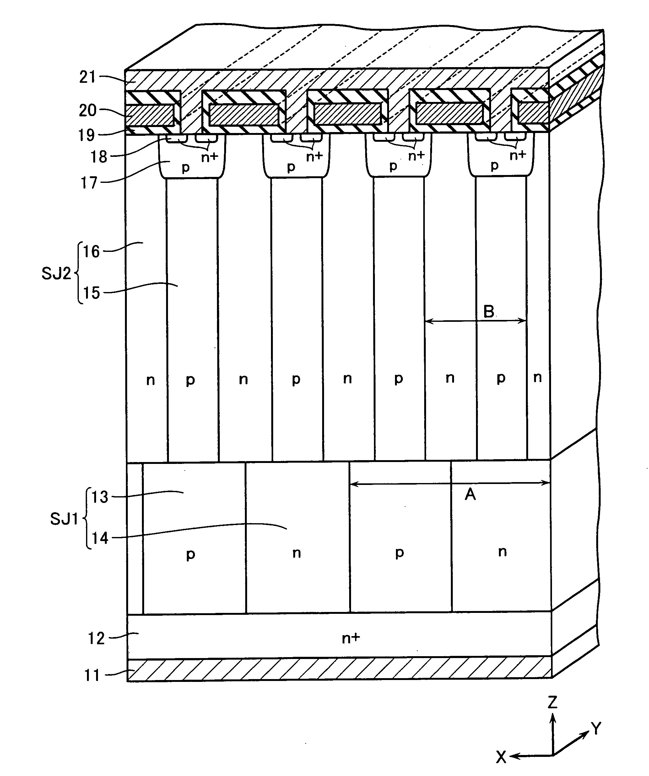
[0035]FIG. 1 is a cross-sectional view schematically showing a structure of a power MOSFET according to a first embodiment of the present invention. This MOSFET includes an n+-type drain layer 12. A lower pillar layer SJ1 is formed on the upper surface of the n+-type drain layer 12, and an upper pillar layer SJ2 is stacked thereon. Thus, the MOSFET adopts a superjunction structure having a drift layer with a two-layered structure of the lower pillar layer SJ1 and the upper pillar layer SJ2.

[0036] The lower pillar layer SJ1 includes lower p-type pillar layers 13 and lower n-type pillar layers 14 formed alternatively at a lateral period A. On the other hand, the upper pillar layer SJ2 includes upper p-type pillar layers 15 and upper n-type pillar layers 16 formed alternatively at a lateral period B smaller than the period A (B14 is connected to the upper n-type pillar layer 16 to form a drift layer successively. In this embodiment, the pillar layers 13, 14, 15, 16 each have a stripe ...

second embodiment

[0054]FIG. 17 is a cross-sectional view schematically showing a structure of a power MOSFET according to a second embodiment of the present invention. The same parts as those in FIG. 1 are omitted from the following detailed description and only different parts are described herein.

[0055] The structure shown in FIG. 17 is the same as the structure of the first embodiment because the upper and lower pillar layers SJ1 and SJ2 are formed in the shape of stripes. It is different from the first embodiment, however, in that the pillar layers SJ1 and SJ2 are arranged such that the directions of extension of the stripe shapes intersect at a right angle. In the structure of the second embodiment, even if an error occurs in alignment of the upper and lower pillar layers SJ1 and SJ2, an increase in on-resistance can be suppressed. In a word, even when the upper and lower pillar layers SJ1 and SJ2 are formed in the shape of stripes and the directions of extension are determined in an identical...

third embodiment

[0056]FIG. 18 is a cross-sectional view schematically showing a structure of a power MOSFET according to a third embodiment of the present invention. The same parts as those in FIG. 1 are omitted from the following detailed description and only different parts are described herein.

[0057] In the structure shown in FIG. 18, the upper pillar layer SJ2 is formed in the shape of stripes similar to those in the above embodiments. On the contrary, the lower pillar layer SJ1 is formed such that the lower p-type pillar layers 13 are buried in the shape of a grid in an n-type layer, which is to be turned intothelowern-typepillarlayers14. Thus, in the lower p-type pillar layers 13, the current path connected to any one of the upper p-type pillar layers 15 is not broken. Accordingly, the on-resistance is prevented from increasing and the process can be simplified.

[0058] The lower p-type pillar layers 13 have a grid formation period A, which is made larger than the lateral period B in the uppe...


PUM


Abstract

First semiconductor pillar layers of a first conduction type and second semiconductor pillar layers of a second conduction type are arranged on a first semiconductor layer of the first conduction type laterally, periodically and alternately at a first period to forma first pillar layer. Third semiconductor pillar layers of the first conduction type and fourth semiconductor pillar layers of the second conduction type are arranged on the first pillar layer laterally, periodically and alternately at a second period smaller than the first period to form a second pillar layer. A semiconductor base layer of the second conduction type is formed on a surface of the fourth semiconductor pillar layer. A semiconductor diffused layer of the first conduction type is formed on a surface of the semiconductor base layer.

Description

CROSS REFERENCE TO RELATED APPLICATION [0001] This application is based on and claims the benefit of priority from prior Japanese Patent Application No. 2005-178834, filed on Jun. 20, 2005, the entire contents of which are incorporated herein by reference. BACKGROUND OF THE INVENTION [0002] 1. Field of the Invention [0003] The present invention relates to a semiconductor device and a method of fabricating the same. More particularly, it relates to a semiconductor device having a superjunction structure with p-type pillar layers and n-type pillar layers buried in a drift layer laterally and alternately, and a method of fabricating the same. [0004] 2. Description of the Related Art [0005] A vertical power MOSFET has an on-resistance greatly dependent on the electrical resistance in a conduction layer (drift layer) thereof. The electrical resistance in the drift layer is determined from its impurity concentration, and the on-resistance can be lowered as the impurity concentration is ma...

Claims


Application Information

Patent Timeline
IPC IPC(8): H01L29/76
CPCH01L29/0634H01L29/7802H01L29/66712H01L29/1095
Inventor SAITO, WATARUOMURA, ICHIRO
Owner KK TOSHIBA
Why Eureka
Try Eureka