Organic electroluminescent display device

a technology of electroluminescent display and organic materials, which is applied in the direction of organic semiconductor devices, semiconductor devices, electric discharge tubes, etc., can solve the problems of reducing image quality, reducing picture quality, and reducing image quality such as blurred outline, depending on the effect of the pixel d

Inactive Publication Date: 2006-12-28
FUJIFILM CORP
View PDF4 Cites 20 Cited by
  • Summary
  • Abstract
  • Description
  • Claims
  • Application Information

AI Technical Summary

Problems solved by technology

In the process of manufacturing such an organic EL display, the upper and lower electrodes can short out so that pixel defects can be produced, due to various causes such as dust contamination, a flaw made by a collision between a vapor deposition mask and a substrate, and a residue caused by insufficient cleaning of a substrate.
Once such pixel defects are visually recognized in a displayed image, they cannot be neglected, and thus the occurrence of defective pixels can significantly reduce the picture quality.
The method disclosed in JP-A No. 2004-279464 has a problem in which a reduction in image quality such as a blurred outline can occur depending on the image.

Method used


Image

  • Organic electroluminescent display device
  • Organic electroluminescent display device
  • Organic electroluminescent display device

Examples


example 1

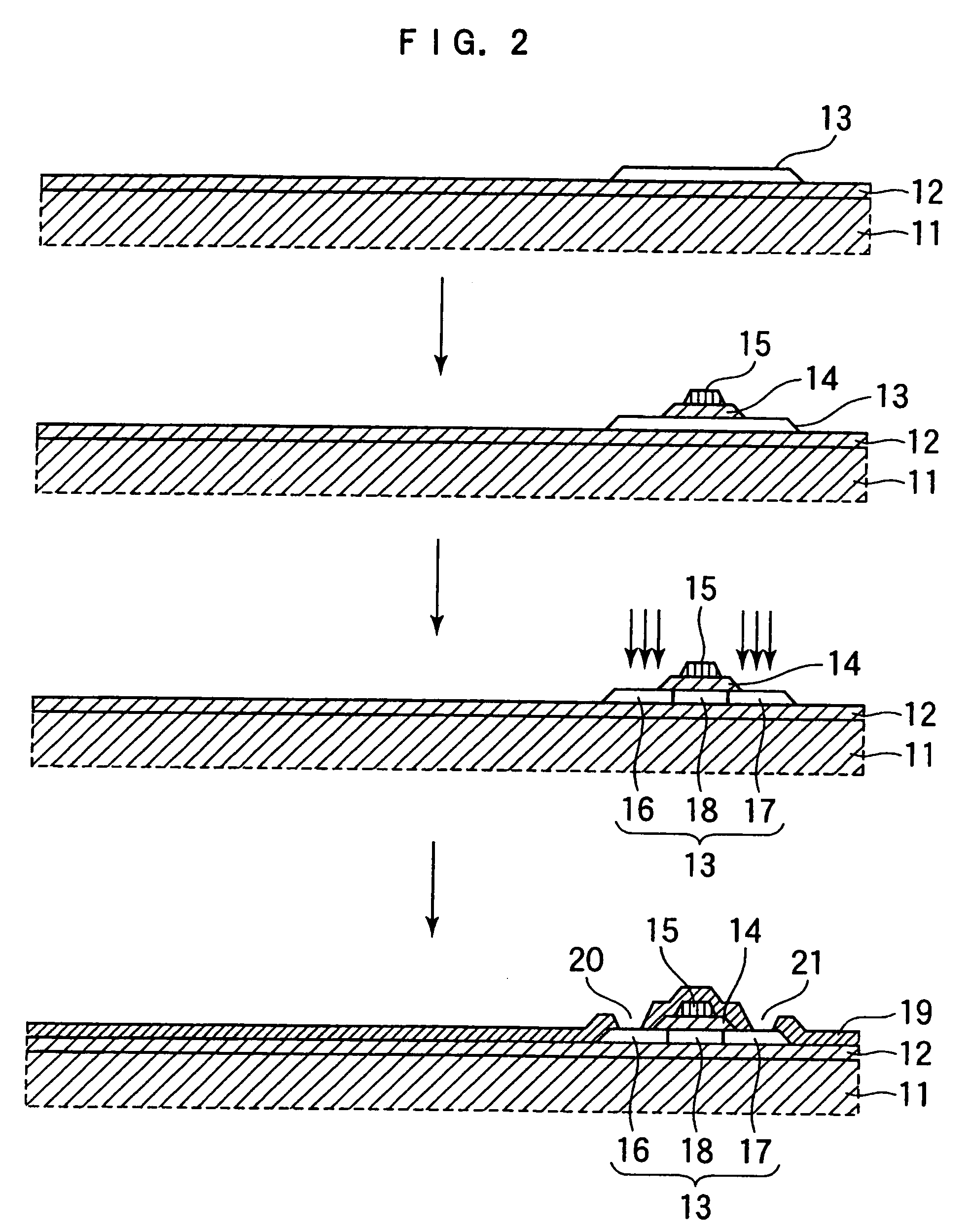
[0054] A bottom emission organic EL display device according Example 1 of the invention is described below with reference to FIGS. 2 to 5.

[0055] After a buffer layer 12 comprising a SiO2 film is first formed on an insulating substrate 11 comprising a glass substrate by a CVD method, a polycrystalline silicon layer is deposited by a CVD method, and then an island polycrystalline silicon layer 13 is formed by a conventional photo-etching process.

[0056] After a SiO2 film is deposited over the entire surface by a CVD method, an AlNd film is deposited by sputtering, and then the SiO2 film and the AlNd film are patterned by a conventional photo-etching process to form a gate insulating film 14 and a gate electrode 15.

[0057] Using the gate electrode 15 as a mask, phosphorus ions are implanted, for example, by ion implantation to form source and drain areas 16 and 17 in the island polycrystalline silicon layer 13 on both sides of the gate electrode 15 and to make the remaining portion a ...

example 2

[0073] A bottom emission organic EL display device according to Example 2 of the invention is described with reference to FIGS. 6 and 7. Plan views only are provided, since the element structure itself is the same as a conventional structure.

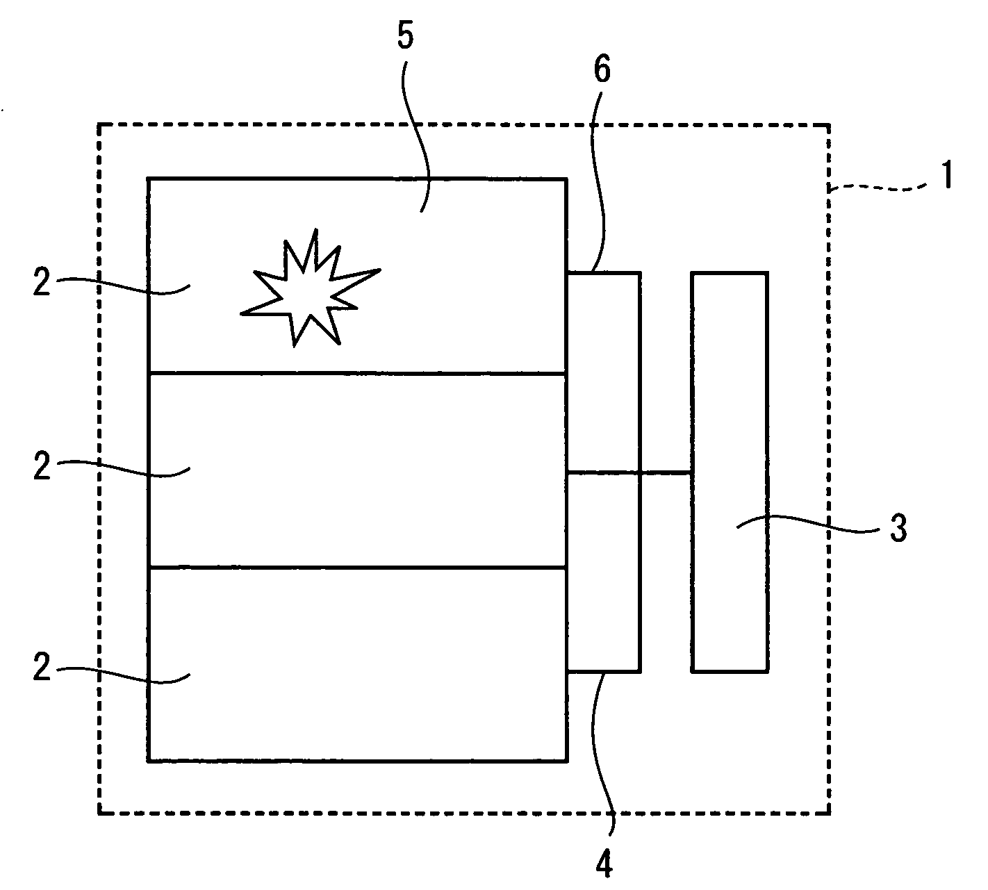
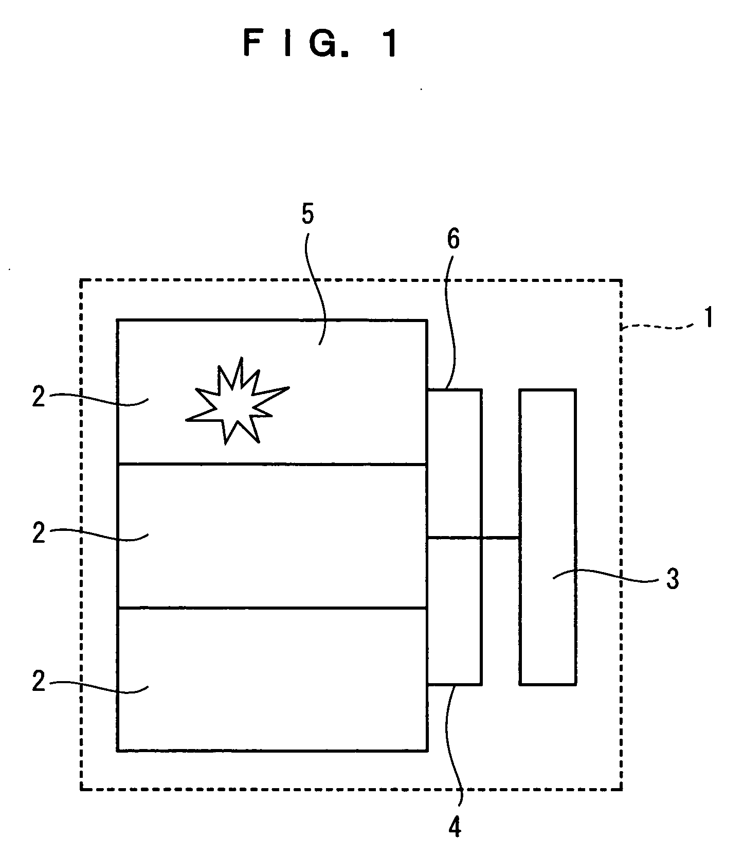
[0074]FIG. 6 is a plan view schematically showing the main part of one sub-pixel according to Example 2 of the invention, in which one conventional sub-pixel structure is segmented into three segmented pixel parts 51 to 53, which are each connected to the same gate line 41, data line 42, and power supply line 43 through segmented pixel circuits 54 to 56 each containing an independent TFT.

[0075]FIG. 7 is an illustration of how to repair when any pixel defect is found. When a pixel defect is found by a lighting test in the same manner as Example 1, all or any of the connections to the gate line 41, the data line 42 and the power supply line 43 is cut by laser fusion cutting such that the TFT of the pixel circuit 55 connected to the segmented pix...

example 3

[0079] A top emission organic EL display device according Example 3 of the invention is described with reference to FIGS. 8 to 10.

[0080] Referring to FIG. 8, a TFT is first formed on an insulating substrate 11 through a buffer layer 12 in the same manner as Example 1. After an interlayer insulating layer19 comprising a SiN film is deposited over the entire surface, contact holes are formed so as to reach source and drain areas 16 and 17, respectively, using a conventional photo-etching process.

[0081] Thereafter, an electrically conductive layer of an Al / Ti / Al multilayer structure is deposited over the entire surface and then patterned by a conventional photo-etching process to form a source electrode 61 also extending onto the TFT part and to form a drain electrode 25.

[0082] As shown in the plan view in the second row, the source electrode 61 is composed of a common source line 62 and four branch lines 63 branched from the line 62. For ease of illustration of the structure of the...


PUM


Abstract

The present invention provides an organic electroluminescent display device, comprising: pixels that are each divided into at least two segments; current supply lines each independently connected to each of the segments; and active elements that are provided per each pixel and control the connection between an organic electroluminescent element and a power supply line, wherein at least one connection line between a defective segment of the segments and the active element is cut.

Description

CROSS-REFERENCE TO RELATED APPLICATION [0001] This application claims priority under 35 USC 119 from Japanese Patent Application No. 2005-155614, the disclosure of which is incorporated by reference herein. BACKGROUND OF THE INVENTION [0002] 1. Field of the Invention [0003] The present invention relates to an organic electroluminescent display device and particularly to an active matrix organic electroluminescent display device characterized by a structure for recovering from a display defect caused by a short-circuit defect due to dust or residues associated with manufacturing processes. [0004] 2. Description of the Related Art [0005] While in recent years, thin flat panel displays such as liquid crystal displays and plasma displays have been widely used as alternatives to CRTs, attention has recently been focused on organic electroluminescent (EL) displays among self-light-emitting flat panel displays. [0006] The organic EL display comprises a large number of organic EL element pi...

Claims


Application Information

Patent Timeline
Patent Type & Authority Applications(United States)
IPC IPC(8): H01J17/00
CPCH01L27/3211H01L27/3248H01L2251/568H01L51/5221H01L2251/5315H01L51/5206H10K59/35H10K59/123H10K50/81H10K2102/3026H10K71/861
Inventor TAKAHASHI, TOSHIRONAKAYAMA, MASAYASATOU, TASUKU
Owner FUJIFILM CORP
Why Eureka
Try Eureka