Semiconductor device and driving method thereof

a technology of magnetic field and driving method, which is applied in the direction of static indicating devices, non-linear optics, instruments, etc., can solve the problems of low yield and inability to take particular measures, and achieve the effects of improving the reliability of transistors, reducing off-current, and reducing the number of transistors

Active Publication Date: 2007-01-04
SEMICON ENERGY LAB CO LTD
View PDF49 Cites 36 Cited by
  • Summary
  • Abstract
  • Description
  • Claims
  • Application Information

AI Technical Summary

Benefits of technology

[0011] Since each of the third TFT and the fourth TFT operates as a switching element, it may be replaced with either an electrical switch or a mechanical switch as long as it can control a current flow. As the switching element, any of a transistor, a diode, and a logic circuit constructed from them can be employed. Further, the first TFT and the second TFT may also be operated as switching elements. In such a case, if the operating point of the first TFT and the first light-emitting element and the operating point of the second TFT and the second light-emitting element are set so as to allow the first TFT and the second TFT to operate in the linear region, variations in the threshold voltage of the first TFT and the second TFT will not affect the display; therefore, a display device with higher image quality can be provided.
[0024] In the invention, various types of transistors may be used, and such transistors may be formed over various types of substrates. Accordingly, the whole circuits may be formed over a glass substrate, a plastic substrate, a single crystalline substrate, an SOI substrate, or any other substrate. By forming the whole circuits over the same substrate, the number of component parts can be reduced to cut cost, as well as the number of connections with the circuit components can be reduced to improve the reliability. Alternatively, a part of the circuits may be formed over one substrate, while the other parts of the circuits may be formed over another substrate. That is, not the whole circuits are required to be formed over the same substrate. For example, a part of the circuits may be formed with transistors over a glass substrate, while the other parts of the circuits may be formed over a single crystalline substrate, so that the IC chip is connected to the glass substrate by COG (Chip-On-Glass) bonding. Alternatively, the IC chip may be connected to the glass substrate by TAB (Tape Automated Bonding) or a printed board. In this manner, by forming a part of the circuits over the same substrate, the number of component parts can be reduced to cut cost, as well as the number of connections with the circuit components can be reduced to improve the reliability. In addition, by forming a portion with a high driving voltage or a high driving frequency, which consumes large power, over different substrates, increase in power consumption can be prevented.

Problems solved by technology

However, in the conventional driving method of a pixel configuration where one pixel has a plurality of sub-pixels, there has been a problem in that if pixels have defects before shipment, any particular measures cannot be taken, which results in a lower yield.
Further, even when pixels have defects after the display device starts to be used, any particular measures cannot be taken.

Method used


Image

  • Semiconductor device and driving method thereof
  • Semiconductor device and driving method thereof
  • Semiconductor device and driving method thereof

Examples


embodiment mode 1

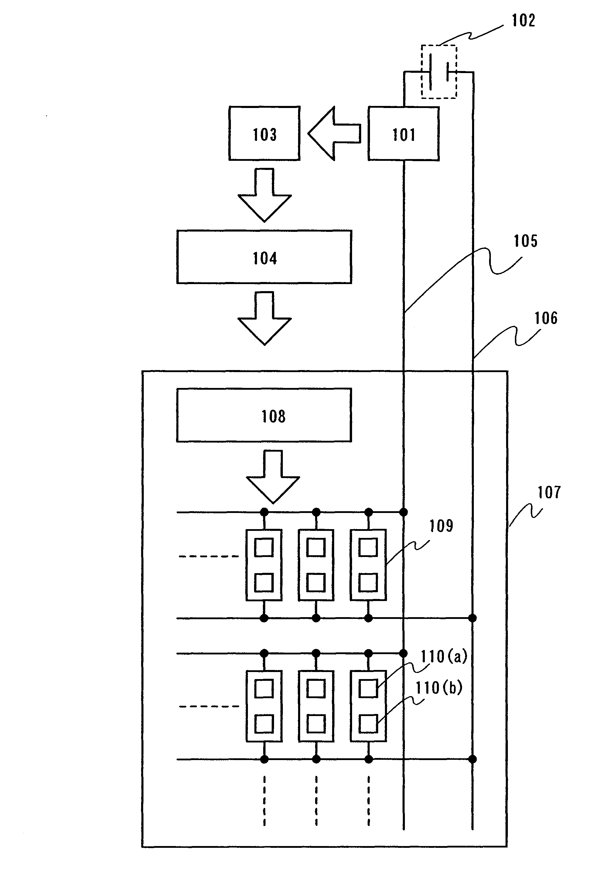
[0103] Description will be made of a display device with a first configuration, with reference to FIG. 1. In FIG. 1, reference numeral 101 denotes a current value detection circuit, 102 denotes a power supply, 103 denotes a compensation circuit, 104 denotes a signal input circuit, 105 denotes a power supply line, 106 denotes a wire, 107 denotes a panel, 108 denotes a driver circuit, 109 denotes a pixel, and 110(a) and 110(b) denote sub-pixels.

[0104] In this semiconductor device, the power supply line 105 is connected to the sub-pixels 110(a) and 110(b) which constitute the pixel 109; the wire 106 is connected to the sub-pixels 110(a) and 110(b) which constitute the pixel 109; the power supply line 105 is connected to a positive side of the power supply 102 through the current value detection circuit 101; a negative side of the power supply 102 is connected to the wire 106; the current value detection circuit 101 outputs a current detected to the compensation circuit 103; the compen...

embodiment mode 2

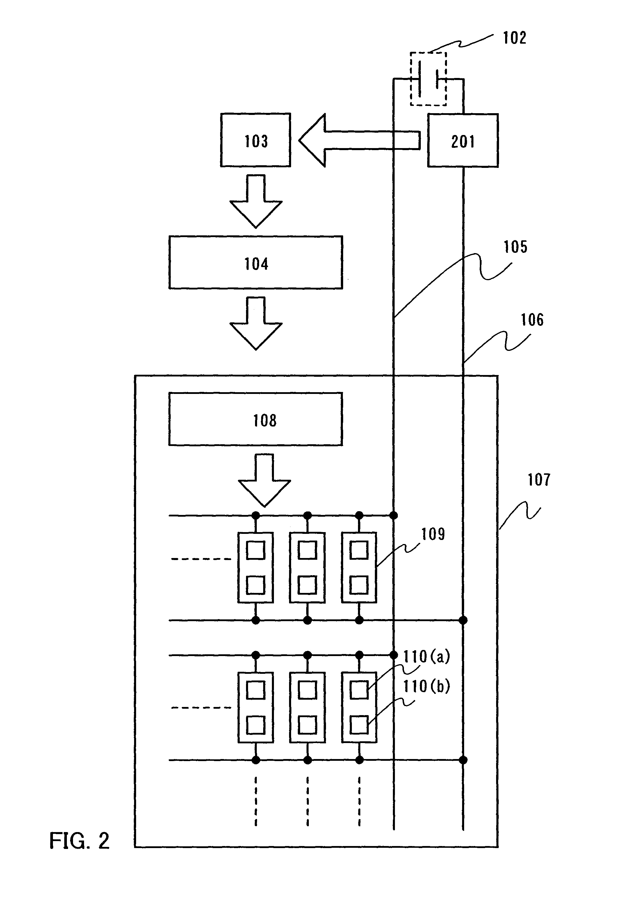
[0121] Description will be made of a display device with a second configuration, with reference to FIG. 2. In FIG. 2, reference numeral 201 denotes a current value detection circuit, 102 denotes a power supply, 103 denotes a compensation circuit, 104 denotes a signal input circuit, 105 denotes a power supply line, 106 denotes a wire, 107 denotes a panel, 108 denotes a driver circuit, 109 denotes a pixel, and 110(a) and 110(b) are sub-pixels.

[0122] In this semiconductor device, the power supply 102 is connected to the sub-pixels 110(a) and 110(b) which constitute the pixel 109; the wire 106 is connected to the sub-pixels 110(a) and 110(b) which constitute the pixel 109; the power supply line 105 is connected to a positive side of the power supply 102; a negative side of the power supply 102 is connected to the wire 106 through the current value detection circuit 201; the current value detection circuit 201 outputs a current detected to the compensation circuit 103; the compensation ...

embodiment mode 3

[0136] Description will be made of an exemplary configuration of the current value detection circuits 101 and 201 described in Embodiment Modes 1 and 2, with reference to FIG. 3.

[0137] In FIG. 3, reference numerals 301 and 302 denote power supply lines, 303 denotes a resistor, 304 denotes a switching element, and 305 denotes an analog-digital converter circuit.

[0138] In this semiconductor device, the power supply line 301 is connected to one terminal of the resistor 303 and one terminal of the switching element 304. The power supply line 302 is connected to the other terminal of the resistor 303, the other terminal of the switching element 304, and an input of the analog-digital converter circuit 305. In addition, the power supply line 301 is connected to the positive side of the power supply 102 (in Embodiment Mode 1) or the negative side thereof (in Embodiment Mode 2), while the power supply line 302 is connected to the power supply line 105 (in Embodiment Mode 1) or the wire 10...


PUM


Abstract

The semiconductor device includes a plurality of pixels each including a plurality of sub-pixels, a power supply line and a plurality of signal lines for operating the plurality of pixels, a driver circuit for outputting signals to the plurality of signal lines, a signal input circuit for controlling the driver circuit, a compensation circuit which determines if a pixel has a normal state, a defective bright spot, or a point defect in the case where a current value detected shows an abnormal value, and accordingly outputs a compensation signal to the signal input circuit, and a current value detection circuit which detects a current value flowing through the power supply line when each sub-pixel is lighted. Thus, a pixel including a sub-pixel which shows an abnormal current value when lighted is compensated by a signal output from the driver circuit.

Description

BACKGROUND OF THE INVENTION [0001] 1. Field of the Invention [0002] The present invention relates to a semiconductor device having a plurality of pixels arranged in matrix, which displays images with a video signal (also referred to as an image signal or a picture signal) input to each of the plurality of pixels, and a driving method thereof. In particular, the invention relates to a semiconductor device having a function of detecting and compensating defective pixels which would be caused in each column, and a driving method thereof. [0003] 2. Description of the Related Art [0004] A driving method is proposed, by which gray scales capable of being displayed on a display screen are increased by providing a plurality of sub-pixels in one pixel (Reference 1: Japanese Patent Laid-Open No. Hei11-73158). For example, in Reference 1, one pixel is constructed from a pluraliuty of sub-pixels, thereby a gray scale which can be expressed with only light emission and non-light emission of one ...

Claims


Application Information

Patent Timeline
Patent Type & Authority Applications(United States)
IPC IPC(8): G09G3/30
CPCG09G3/006G09G3/2007G09G3/3266G09G2330/12G09G2330/08G09G2330/10G09G3/3283G02F1/133G09G3/20G09G3/36
Inventor UMEZAKI, ATSUSHIKIMURA, HAJIMEYAMAZAKI, SHUNPEI
Owner SEMICON ENERGY LAB CO LTD
Why Eureka
Try Eureka