Circular symmetrical microlens/color filter array shift and digital lens shading correction

a microlens and filter array technology, applied in the field of imaging systems, can solve the problems of large (up to 50%) degradation of light intensity across the array, significant shift of individual pixels within the pixel array, and large (up to 50%) reduction of light intensity

Active Publication Date: 2007-02-08
APTINA IMAGING CORP
View PDF10 Cites 97 Cited by
  • Summary
  • Abstract
  • Description
  • Claims
  • Application Information

AI Technical Summary

Benefits of technology

[0013] Exemplary embodiments of the invention include an image sensor formed with shifts among the optical parts of the sensor and the photosensitive parts of the sensor. Exemplary methods of calculating the desired shift are described and include a circular, symmetric design technique. The exemplary method can also be used to calculate a correction coefficient for performing shading correction on signals that are output from the array and digitized.

Problems solved by technology

One of the difficulties in designing and implementing imaging systems is the optimization of individual pixels within a pixel array.
The problem becomes significant in imaging applications receiving non-telecentric light, where different pixels of the array are illuminated with light having different chief ray angles, depending on the location of the pixel in the array.
In addition, the relative illumination of the imaging lens results in large (up to 50%) degradation of light intensity across the array.
Imaging lenses that have non-linear behavior of the chief ray angle as a function of image height, however, have difficulty in using the orthogonal method.
Specifically, the microlens-color filter locations and the lens shading correction can not be fully optimized for the imaging lens, which results in non-uniform signal response as well as color distortion.
As stated above, traditional methods for optimizing these arrays are not sufficient.

Method used


Image

  • Circular symmetrical microlens/color filter array shift and digital lens shading correction
  • Circular symmetrical microlens/color filter array shift and digital lens shading correction
  • Circular symmetrical microlens/color filter array shift and digital lens shading correction

Examples


Embodiment Construction

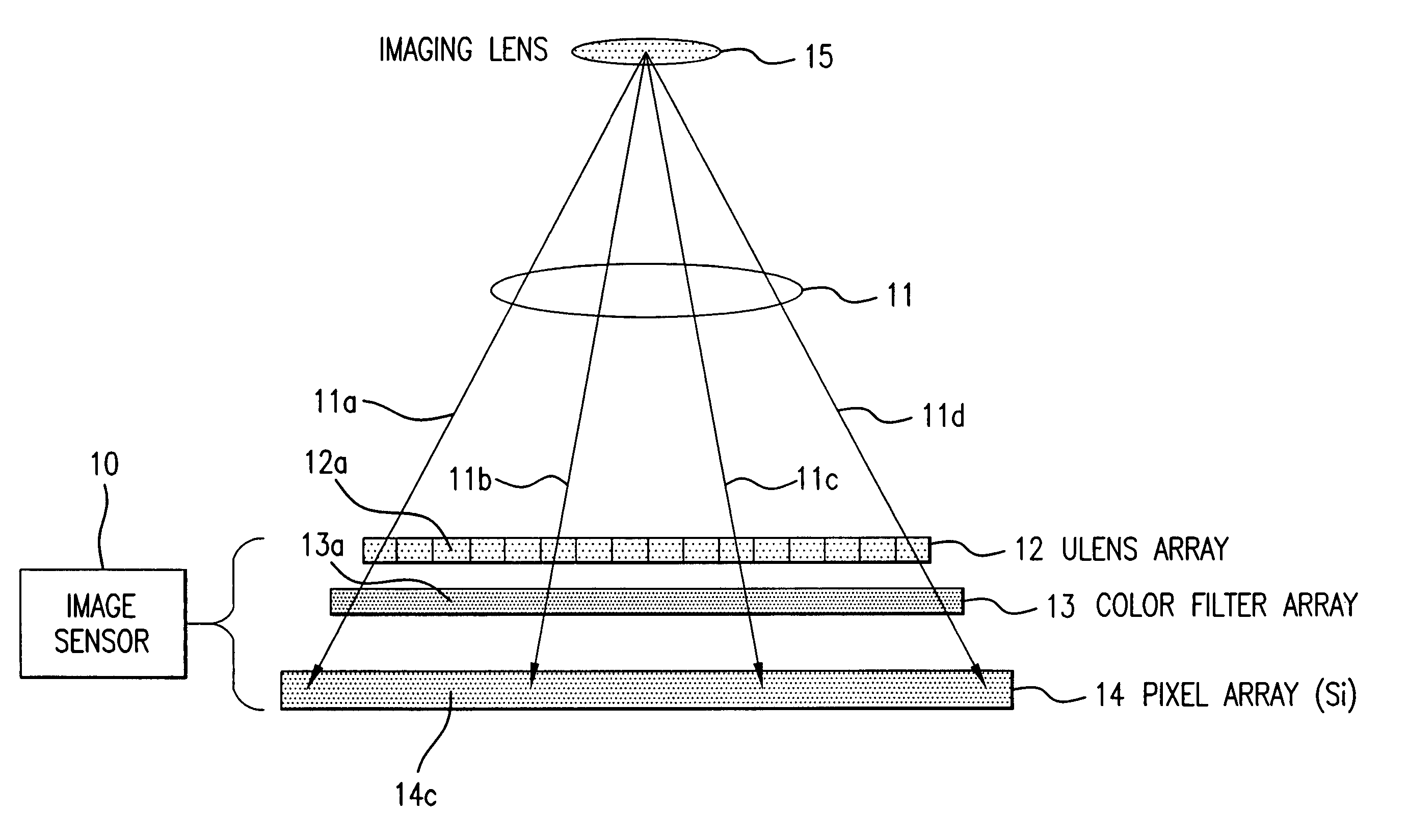
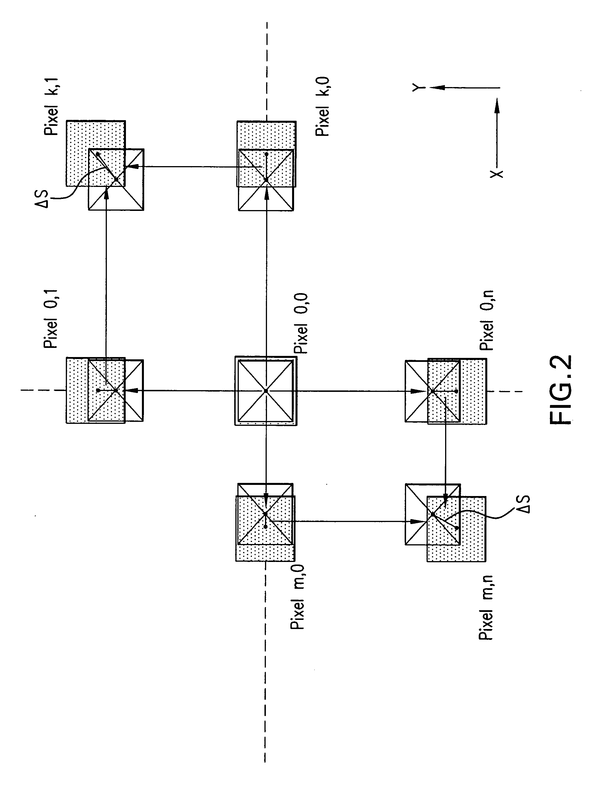
[0027] The term “pixel,” as used herein, refers to a photo-element unit cell containing a photosensor device and associated structures for converting photons to an electrical signal. For purposes of illustration, a representative three-color R, G, B pixel array is described herein; however, the invention is not limited to the use of an R, G, B array, and can be used with other color arrays, one example being C, M, Y, K (which represents cyan, magenta, yellow and black color filters). In addition, the invention can also be used in a mono-chromatic array where just one color is sensed by the array. Accordingly, the following detailed description is not to be taken in a limiting sense, and the scope of the present invention is defined not by the illustrative embodiments, but by the scope of the appended claims.

[0028] It should also be understood that, taken alone, a pixel does not distinguish one incoming color of light from another and its output signal represents only the intensity ...


PUM


Abstract

An image sensor formed with shifts among the optical parts of the sensor and the photosensitive parts of the sensor. Exemplary methods of calculating the desired shift are described and include a circular, symmetric design for the shift. The exemplary methods can also be used to calculate a correction coefficient for performing shading correction on signals that are output from the array and digitized.

Description

FIELD OF THE INVENTION [0001] The invention relates generally to improved imaging systems using image sensor pixel arrays, and more particularly, to optimizing a shift among optical parts, including a microlens and color filter array, in the imaging system. BACKGROUND OF THE INVENTION [0002] Image sensors receive light into an array of photosensitive pixels. Each pixel may be formed of a number of cooperating elements including, for example, a lens, often called a “microlens,” a color filter which can block incoming light of a particular color(s) from reaching the photosensitive portion, and the photosensitive portion itself. These elements are typically formed on different physical levels of a substrate. Traditionally, the elements of the pixels should have their centers substantially exactly aligned. That is, the microlens, the color filter, and the photosensitive portion should each be substantially coaxial. [0003] One of the difficulties in designing and implementing imaging sys...

Claims


Application Information

Patent Timeline
Patent Type & Authority Applications(United States)
IPC IPC(8): H04N5/225
CPCH04N5/3572H04N5/2254H04N25/61H04N25/70
Inventor AGRANOV, GENNADIY A.
Owner APTINA IMAGING CORP
Why Eureka
Try Eureka