Methods and apparatus for integrating large and small lot electronic device fabrication facilities

a technology of electronic devices and fabrication facilities, applied in the field of electronic device manufacturing, can solve the problems of increasing the processing time of substrates, compounding the above problems,

Active Publication Date: 2007-03-15
APPLIED MATERIALS INC
View PDF98 Cites 20 Cited by
  • Summary
  • Abstract
  • Description
  • Claims
  • Application Information

AI Technical Summary

Problems solved by technology

The above problem may further compound with longer substrate processing times when performing individual process steps at process or metrology tools.

Method used


Image

  • Methods and apparatus for integrating large and small lot electronic device fabrication facilities
  • Methods and apparatus for integrating large and small lot electronic device fabrication facilities
  • Methods and apparatus for integrating large and small lot electronic device fabrication facilities

Examples


Embodiment Construction

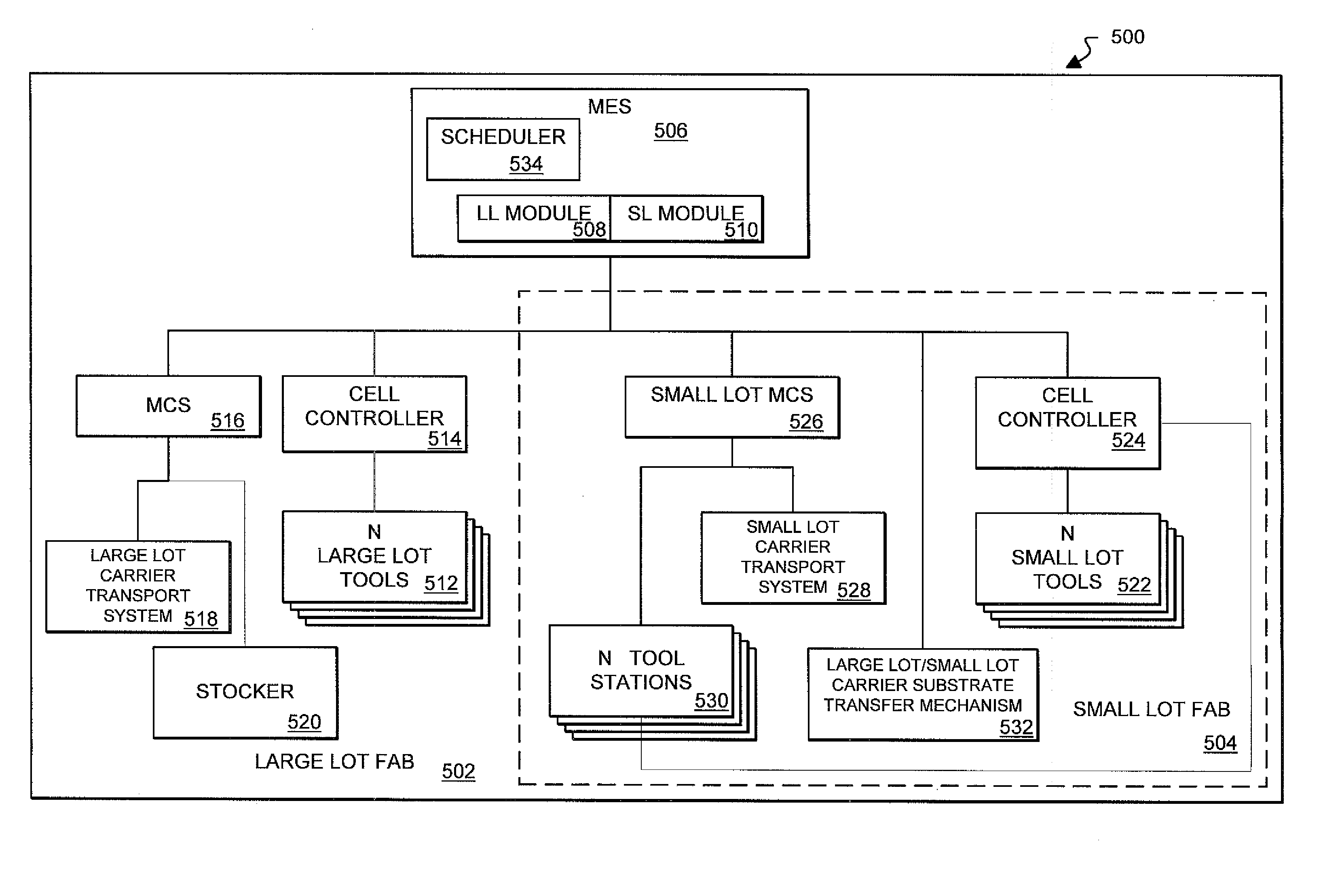
[0026] Aspects of the present invention overcome the drawbacks of the prior art by providing a Fab that uses small lot sized carriers (hereinafter referred to as a “small lot Fab”) that may be transparently integrated into an existing Fab that uses large lot sized carriers (hereinafter referred to as a “large lot Fab”). As used herein, the term “small lot size” carrier or “small lot” carrier may refer to a carrier that is adapted to hold fewer substrates than a conventional “large lot size” carrier which typically holds thirteen or twenty-five substrates. As an example, a small lot size carrier may be adapted to hold five or less substrates. In some embodiments, other small lot size carriers may be employed (e.g., small lot size carriers that hold one, two, three, four or more than five substrates, but less than that of a large lot size carrier). In general, each small lot size carrier may hold too few substrates for human transport of carriers to be viable within a semiconductor de...


PUM


Abstract

In at least one aspect, the invention provides an electronic device fabrication facility (Fab) that uses small lot carriers that may be transparently integrated into an existing Fab that uses large lot carriers. A manufacturing execution system (MES) may interact with the inventive small lot Fab as if the small lot Fab is any other Fab component in an existing large lot Fab without requiring knowledge of how to control small lot Fab components (e.g., beyond specifying a processing recipe). A small lot Fab according to the present invention may encapsulate the small lot Fab's internal use of small lot components and present itself to a large lot Fab's MES as if the small lot Fab is a component that uses large lot carriers.

Description

[0001] This application is a continuation of and claims priority to U.S. patent application Ser. No. 10 / 981,131, filed Nov. 4, 2004 and entitled “Method And Apparatus For Integrating Large And Small Lot Electronic Device Fabrication Facilities” which claims priority to U.S. Provisional Patent Application Ser. No. 60 / 518,583 filed Nov. 6, 2003 and entitled “Single Wafer Software Integration”. Each of these applications is hereby incorporated herein by reference in its entirety for all purposes. RELATED APPLICATIONS [0002] The present application is related to the following commonly-assigned, co-pending U.S. Patent Applications, each of which is hereby incorporated herein by reference in its entirety for all purposes: [0003] U.S. patent application Ser. No. 10 / 650,310, filed Aug. 28, 2003 and titled “System For Transporting Substrate Carriers” (Attorney Docket No. 6900); [0004] U.S. patent application Ser. No. 10 / 764,982, filed Jan. 26, 2004 and titled “Methods and Apparatus for Trans...

Claims


Application Information

Patent Timeline
Patent Type & Authority Applications(United States)
IPC IPC(8): G06F19/00H01L21/68B65G49/07G05B19/418H01L21/00
CPCG05B19/41845G05B2219/31001G05B2219/45031G05B2219/31372G05B2219/31276Y02P90/02H01L21/68
Inventor PURI, AMITABHDUFFIN, DAVIDENGLHARDT, ERIC A.
Owner APPLIED MATERIALS INC
Why Eureka
Try Eureka