Electron emission display

a technology of electron beam and display screen, which is applied in the direction of discharge tube/lamp details, cathode ray tube/electron beam tube, discharge tube luminescnet screen, etc., can solve the problems of hindering the correct expression of color, deteriorating display quality, and difficulty in completely emitted electron beam in a straight manner, so as to prevent or reduce the distortion of electron beam and the deterioration of display quality

Inactive Publication Date: 2007-05-03
SAMSUNG SDI CO LTD
View PDF6 Cites 0 Cited by
  • Summary
  • Abstract
  • Description
  • Claims
  • Application Information

AI Technical Summary

Benefits of technology

[0011] Aspects of the present invention provide an electron emission display which draws out charges on a surface of spacers to prevent or reduce the distortion in electron beams and the deterioration in the display quality due to charging of the spacers.

Problems solved by technology

However, during operation of the electron emission display, it is difficult to completely emit the electron beams in a straight manner.
The distortion in the trajectories of the electron beams hinders the correct expression of color in areas of the phosphor layers around the spacers.
Accordingly, in the areas of a screen around the spacers, the display quality deteriorates.

Method used


Image

  • Electron emission display
  • Electron emission display
  • Electron emission display

Examples


Embodiment Construction

[0023] Reference will now be made in detail to the aspects of the present invention, examples of which are illustrated in the accompanying drawings, wherein like reference numerals refer to the like elements throughout. The aspects are described below in order to explain the present invention by referring to the figures.

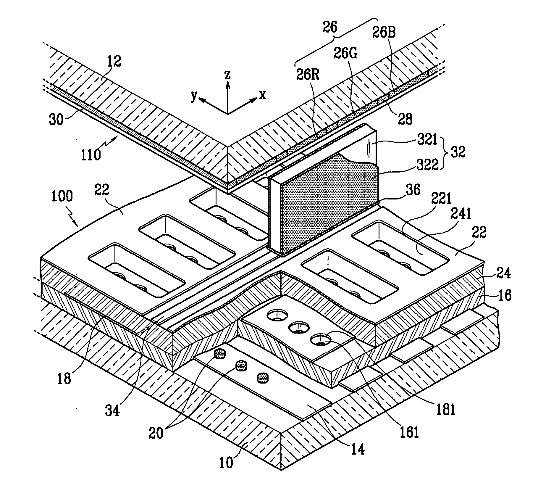
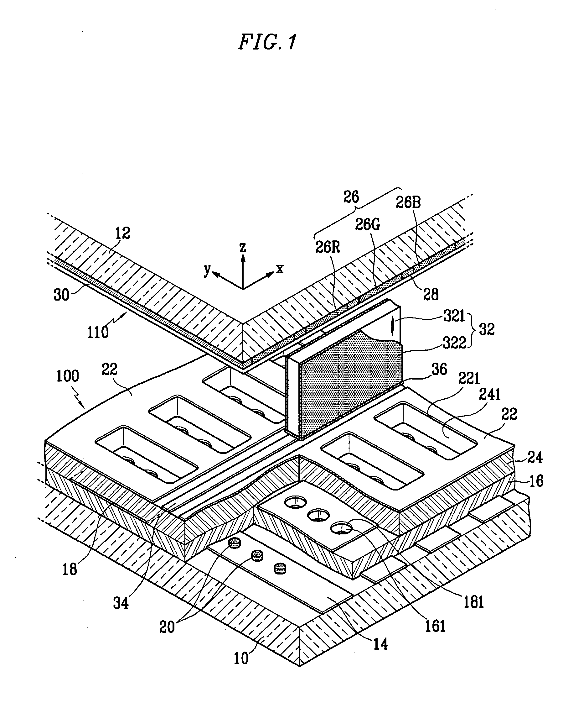
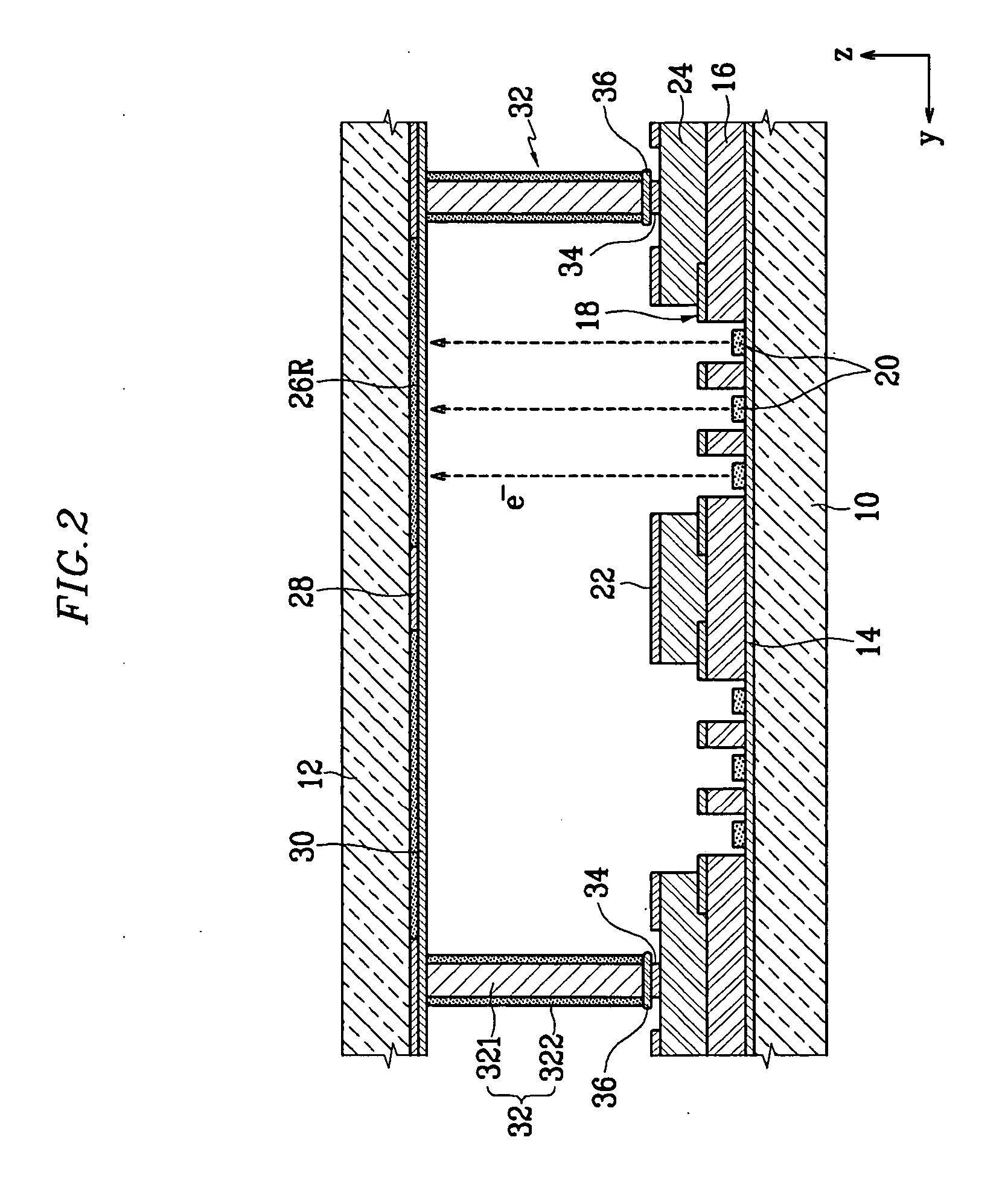
[0024]FIGS. 1 and 2 are a partial exploded perspective view and a partial sectional view of electron emission display according to an aspect of the present invention, respectively. Although not required in all aspects, an FEA type electron emission display is shown in FIGS. 1 and 2.

[0025] As shown in FIGS. 1 and 2, the electron emission display 1 includes parallel first and second substrates 10 and 12 facing each other by a predetermined distance. A sealing member (not shown) is provided at the peripheries of the first and the second substrates 10 and 12 to seal them to one another. Once sealed, the inner space thereof is evacuated to about 10−6 torr. Accordingly, ...


PUM


Abstract

An electron emission display includes first and second substrates facing each other, electron emission regions to emit electrons and formed on the first substrate, and driving electrodes formed on the first substrate to use in the control of the emission of electrons from the electron emission regions. Phosphor layers are formed on a surface of the second substrate. An anode electrode is placed on a surface of the phosphor layers. Spacers are mounted between the first and the second substrates. Antistatic electrodes are placed over the first substrate such that the antistatic electrodes are insulated from the driving electrodes, and electrically connected to the spacers.

Description

CROSS-REFERENCE TO RELATED APPLICATION [0001] This application claims the benefit of Korean Application No. 2005-103350, filed on Oct. 31, 2005 in the Korean Intellectual Property Office, the disclosure of which is incorporated herein by reference. BACKGROUND OF THE INVENTION [0002] 1. Field of the Invention [0003] Aspects of the present invention relate to an electron emission display. In particular, aspects of the present invention relate to an electron emission display which has spacers mounted within a vacuum vessel to withstand the pressure applied thereto. [0004] 2. Description of the Related Art [0005] Generally, electron emission elements are classified into different types depending upon the types of electron sources. These include a first type using a hot cathode and a second type using a cold cathode. The second type electron emission elements using a cold cathode include a field emitter array (FEA) type, a surface conduction emission (SCE) type, a metal-insulator-metal (...

Claims


Application Information

Patent Timeline
Patent Type & Authority Applications(United States)
IPC IPC(8): H01J63/04H01J1/62
CPCH01J29/06H01J29/864H01J31/127H01J2329/864H01J2329/8645H01J2329/8655H01J2329/866
Inventor JUNG, KYU-WONKIM, IL-HWAN
Owner SAMSUNG SDI CO LTD
Why Eureka
Try Eureka