Collection optics for led array with offset hemispherical or faceted surfaces

a technology of hemispherical or faceted surfaces and collection optics, which is applied in the direction of instruments, lighting and heating apparatus, semiconductor devices for light sources, etc., can solve the problems of inability to efficiently efficiently use simple plano-convex lenses, complex aspherical optics, and often too expensive and/or expensive tooling, etc., to achieve the effect of improving the collection efficiency of optics

Active Publication Date: 2007-05-17
SILICON VALLEY BANK
View PDF99 Cites 11 Cited by
  • Summary
  • Abstract
  • Description
  • Claims
  • Application Information

AI Technical Summary

Benefits of technology

[0011] While not intended for imaging applications, this approach is a

Problems solved by technology

The problem with the configuration in FIG. 1 is that the spherical design of each lens 16 assumes that the LED 12 is a point source of light.
However, in reality LEDs are not point sources of light.
Therefore, for some types of light sources, a single spherical lens 22 is an inadequate optic because it does not adequately gather or collect the disparate light so that it is mo

Method used


Image

  • Collection optics for led array with offset hemispherical or faceted surfaces
  • Collection optics for led array with offset hemispherical or faceted surfaces
  • Collection optics for led array with offset hemispherical or faceted surfaces

Examples


Embodiment Construction

[0022] Representative embodiments of the present invention are shown in FIGS. 3-7, wherein similar features share common reference numerals.

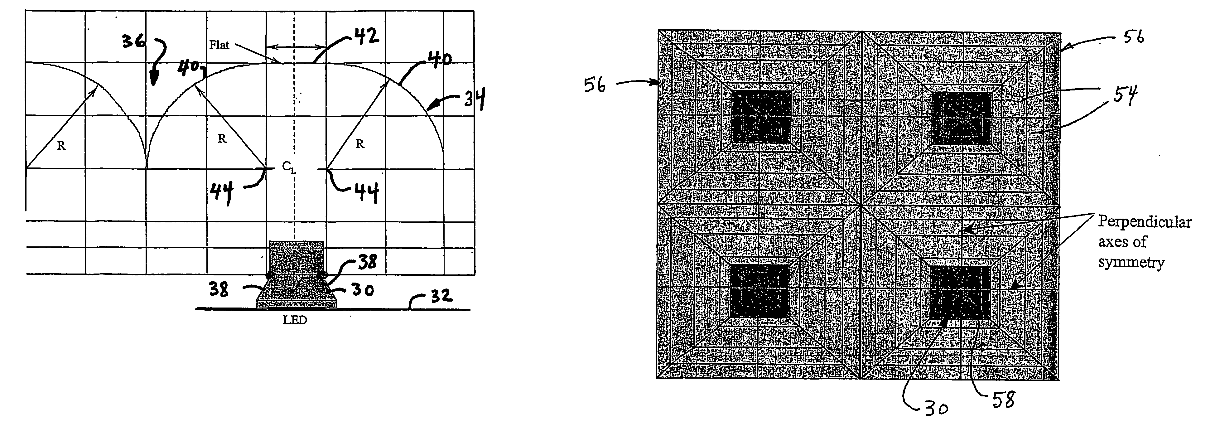
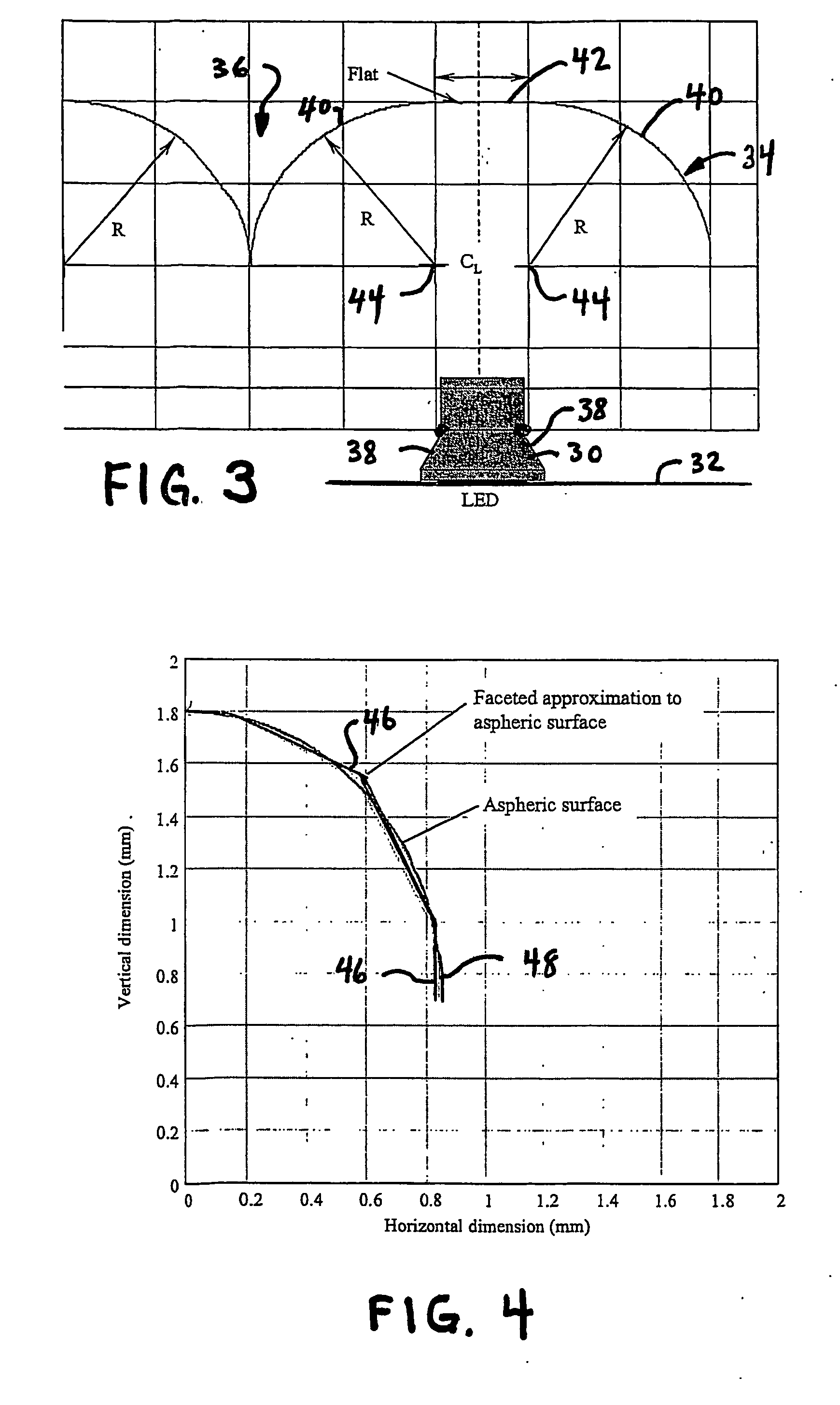
[0023] More specifically, FIG. 3 shows an LED 30 mounted on a circuit board 32 with an associated lens 34 from an array that may comprise, for example, one thousand (1,000) LED's. Each LED 30 typically emits disparate light from the sides 38 so that the light is widely dispersed. In order to more effectively collect the light, lens 34 is formed of a compound shape that includes a curved surfaces 40 separated by a flat surface 42. Curved surfaces 40 may have a spherical or offset aspheric shape, although in FIG. 3 a spherical surface is shown. Lens 34 is centered about center line CL extending through LED 30 so that light from each side 38 of LED 30 is projected into the respective curved surface 40 on that side. Each curved surface 40 is centered about a radius R extending from a center point 44. Each radius R extends from center point 44 that ...


PUM


Abstract

An array of LEDs (30) is provided having a lens array (34) for collecting divergent light from each LED (30). Each lens (34) in the array is associated with a respective LED (30) and has a compound shape including a curved surface (40) that may be spherical or may have an offset aspherical shape. The curved surfaces (40) are centered about each side of its associated LED (30). The lens (34) may alternatively include faceted surfaces (46) that approximate the curved lens surface.

Description

[0001] This invention claims the benefit of co-pending U.S. Provisional Application No. 60 / 516,382, entitled “Collection Optics for Led Array with Offset Hemispherical or Faceted Surfaces”, filed Oct. 31, 2003, the entire disclosure of which is hereby incorporated by reference as if set forth in its entirety for all purposes.BACKGROUND OF THE INVENTION [0002] Solid state lighting devices such as, for example, light emitting diodes (LEDs) are used for a number of applications. One type of such solid state lighting device is disclosed in International Patent Application No. PCT / US03 / 14625, filed May 28, 2003, entitled High Efficiency Solid-State Light Source And Methods Of Use And Manufacture, the details of which are hereby incorporated by reference. [0003] Arrays of light-emitting diodes (LEDs) are used for many purposes. For example, arrays of LEDs are sometimes used in conjunction with arrays of lenses. The lens arrays are used to collect and collimate the light from the array of ...

Claims


Application Information

Patent Timeline
IPC IPC(8): F21V5/00H01L33/58
CPCF21V5/007F21V5/04F21Y2101/02G02B3/0056G02B5/045H01L33/58F21Y2115/10
Inventor ANDERSON, DUWAYNE R.JASMIN, ROLAND
Owner SILICON VALLEY BANK
Why Eureka
Try Eureka