

Surface Plasmon Devices
a surface plasmon and plasmon technology, applied in the direction of optical waveguide light guide, nanotechnology, instruments, etc., can solve the problems of inability to operate at terahertz frequencies or higher, limited device speed, and relatively expensive fabrication of semiconductor-based devices
- Summary
- Abstract
- Description
- Claims
- Application Information
AI Technical Summary
Problems solved by technology
Method used
Image

Examples
Embodiment Construction
[0088] The following description is presented to enable one of ordinary skill in the art to make and use the invention and is provided in the context of a patent application and its requirements. Various modifications to the described embodiments will be readily apparent to those skilled in the art and the generic principles herein may be applied to other embodiments. Thus, the present invention is not intended to be limited to the embodiment shown but is to be accorded the widest scope consistent with the principles and features described herein.
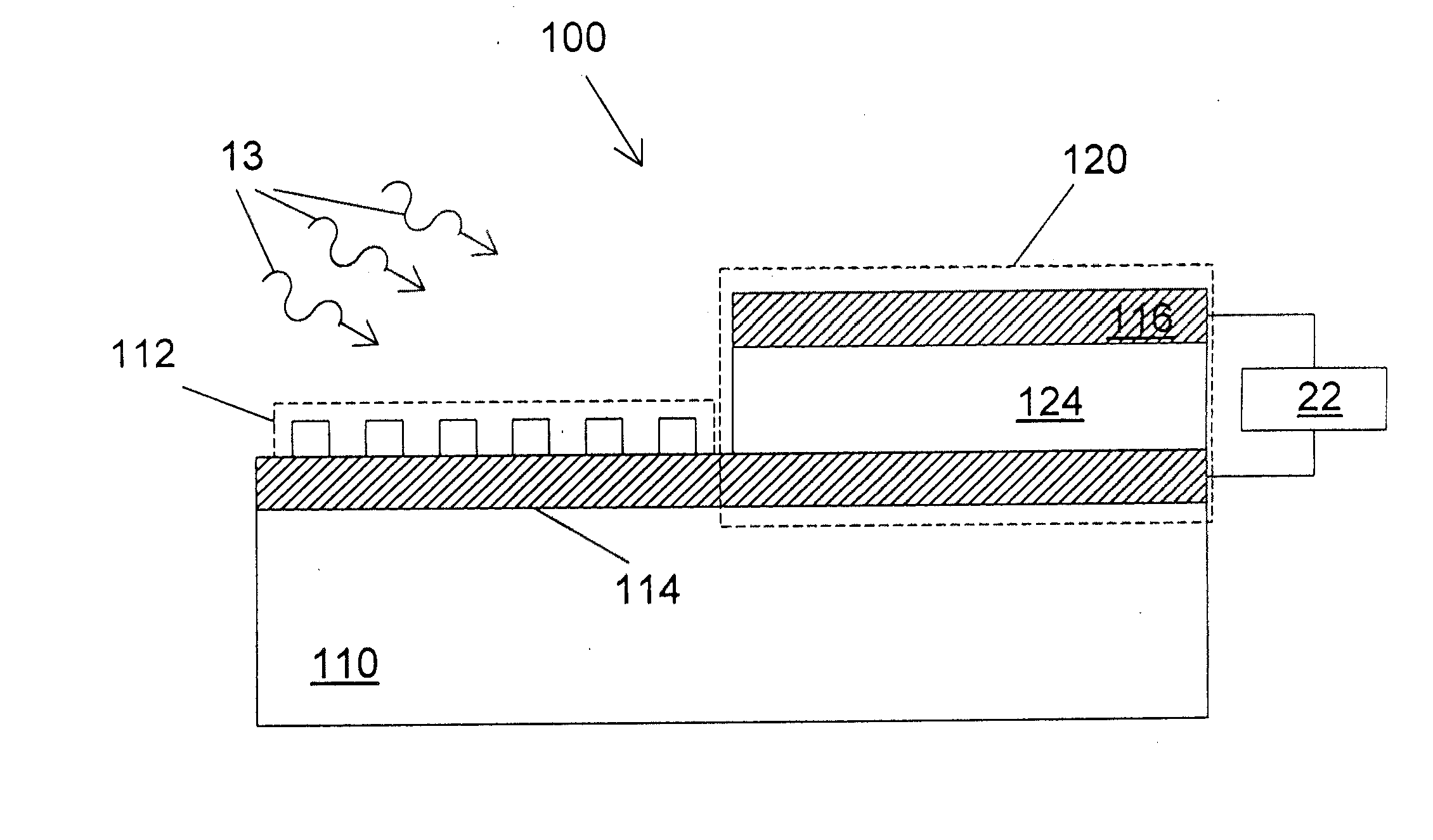
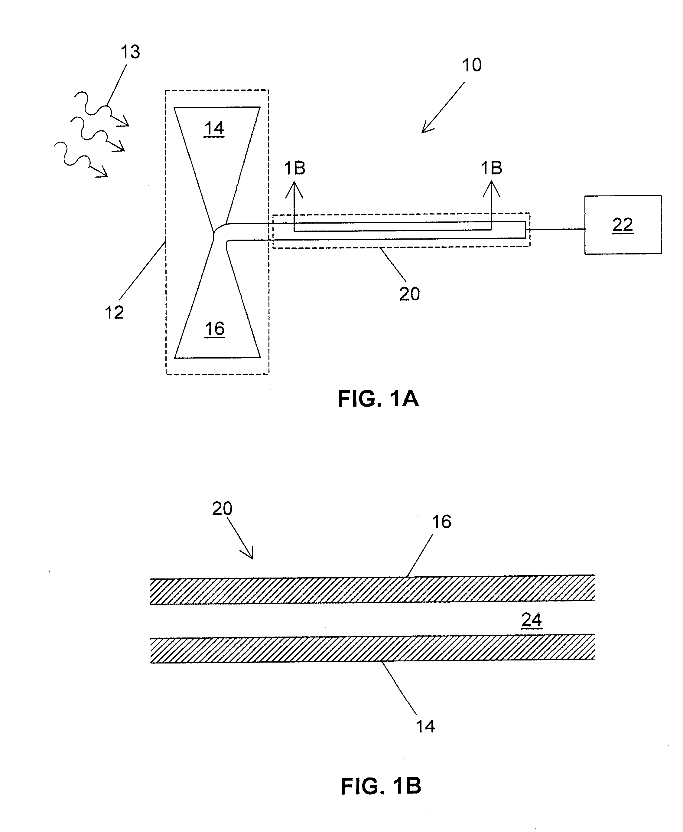
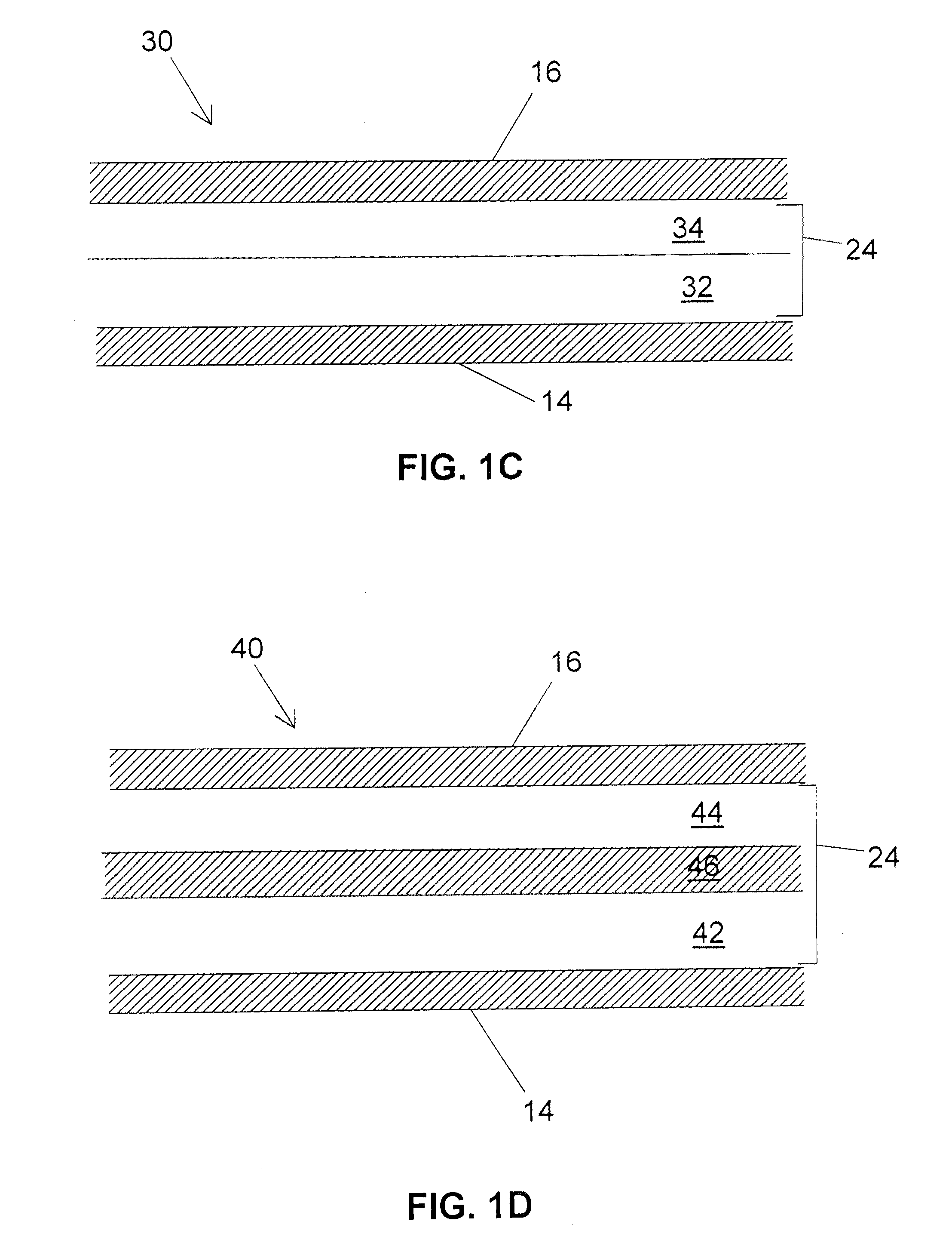
[0089] Although the aforedescribed prior art devices and theoretical disclosures regarding sophisticated manipulation of surface plasmons, such as stimulated emission and stimulated absorption, have been made over the past twenty-five years, the Applicants are unaware of presently available, practical devices that actually allow such manipulations. Recent progress in tunneling junction technology by the assignee of the present application ...
PUM
 Abstract
Description
Claims
Application Information