Waveguide path coupling-type photodiode

a waveguide path and photodiode technology, applied in the field of photodiodes, can solve the problems of poor light absorption efficiency on the surface layer of the semiconductor, high speediness, and difficult to achieve high sensitivity, and achieve low power consumption, high integration, and efficient optoelectric conversion

Active Publication Date: 2010-05-13
NEC CORP +1
View PDF4 Cites 56 Cited by
  • Summary
  • Abstract
  • Description
  • Claims
  • Application Information

AI Technical Summary

Benefits of technology

[0037]The photodiode of the present invention allows the light having propagated through the optical waveguide path core to be effectively entrapped into the light absorption layer. And, the efficient optoelectric conversion is enabled even though the junction area is very small. Further, the photodiode, which is small in the volume of the light absorption layer, and

Problems solved by technology

However, this technique, which enables the high speediness, is poor in a light absorption efficiency on the surface layer of the semiconductor.
And, the high sensitivity is difficult to attain.
However, reducing the junction area causes a utilization efficiency of the signal light to lower.
As a result, an operational speed lowers.
However, in the case of employing the optoelectronic coupler described in the Patent document 4 as an MSM type light receiving element, reducing an irradiation area of the incident light for a purpose of reducing the electric capacity of the depletion layer leads to a decline in the intensity (S/N) of the detection signal.
However, the point of reducing

Method used


Image

  • Waveguide path coupling-type photodiode
  • Waveguide path coupling-type photodiode
  • Waveguide path coupling-type photodiode

Examples


embodiment 1

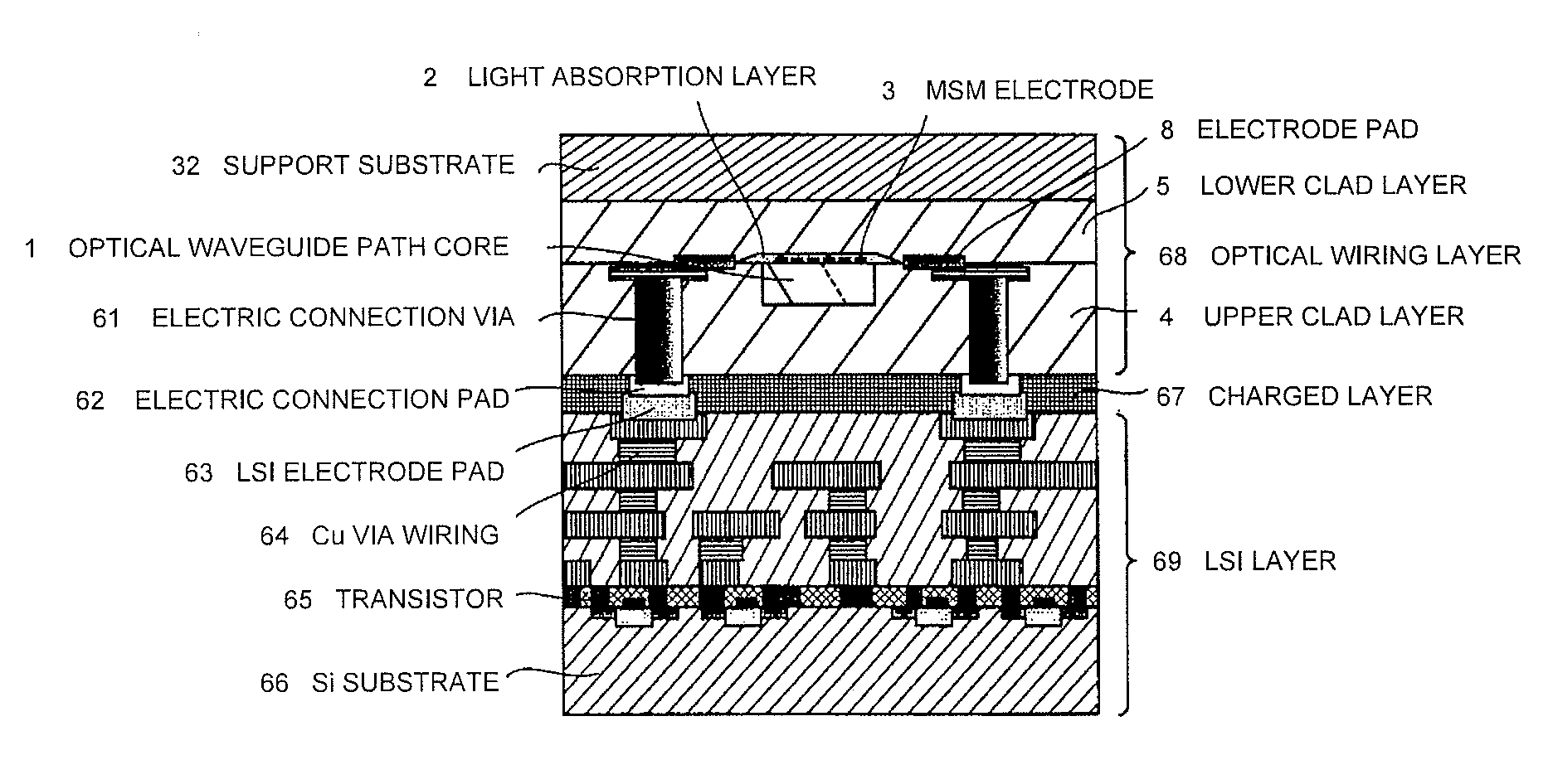
[0091]Each of FIG. 1 to FIG. 3 is a view for explaining the first embodiment of the present invention. FIG. 1 is a cross sectional view. FIG. 2 is a plan. FIG. 3 is a partially enlarged view of FIG. 2.

[0092]Additionally, this embodiment is an example of the MSM photodiode.

[0093]This waveguide path coupling-type photodiode is one formed on one part of the semiconductor layer of which the surface has been insulated, for example, SOI (Silicon-on-Insulator). That is, the clad layer is formed so as to surround an optical waveguide path core 1. Additionally, for convenience, in FIG. 1, the clad layer being positioned on the upper side of the optical waveguide path core 1 is called an upper clad layer 4. The clad layer being positioned on the lower side of the optical waveguide path core 1 is called a lower clad layer 5. As can be seen from FIG. 1, the semiconductor light absorption layer 2 is formed in the boundary portion (interface portion) between the optical waveguide path core 1 and ...

embodiment 2

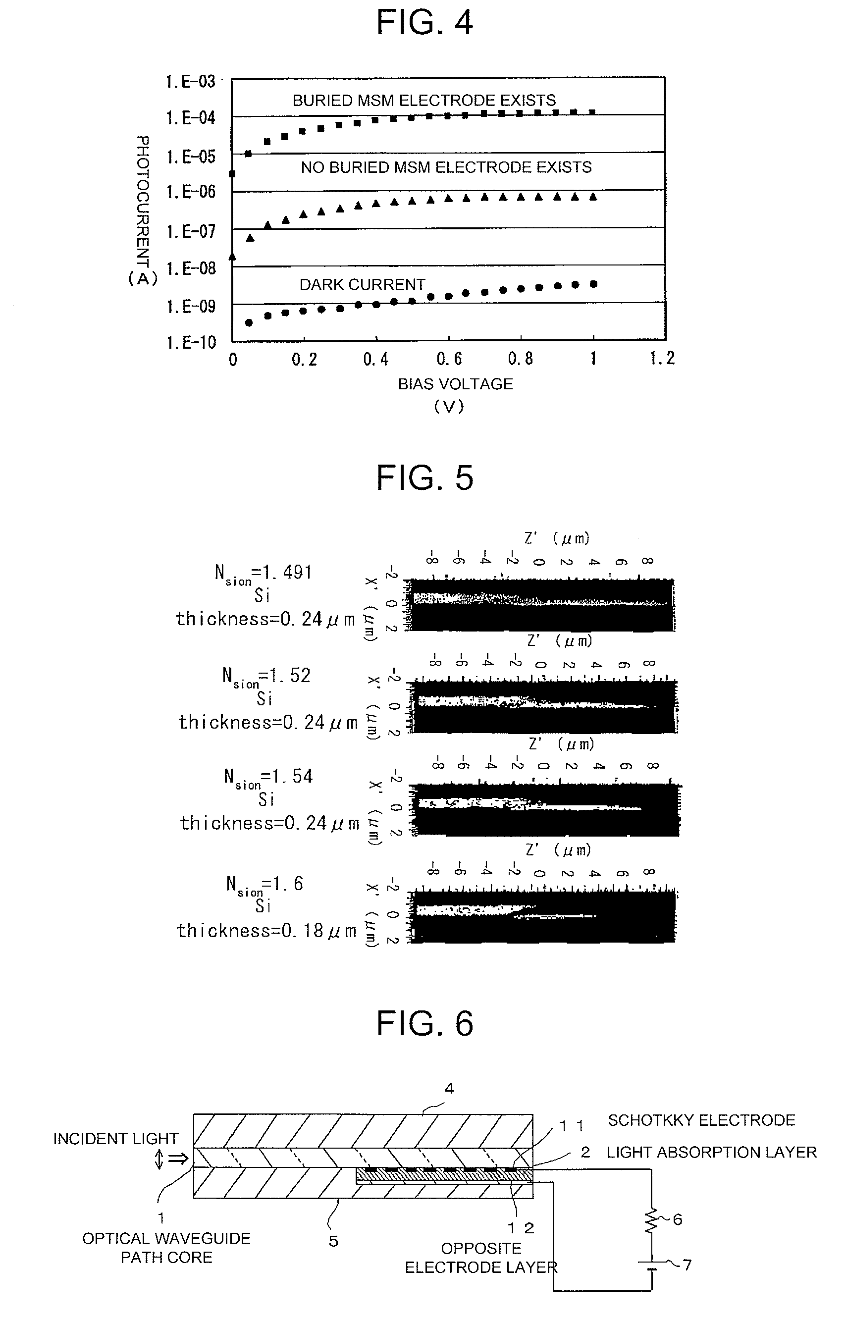
[0116]FIG. 6 is a cross sectional view illustrating the second embodiment of the present invention.

[0117]This embodiment is an example of the Schottky junction type photodiode.

[0118]This waveguide path coupling-type photodiode, similarly to the case of the first embodiment, has the semiconductor light absorption layer 2 formed adjacently to the optical waveguide path core 1. Further, similarly to the case of the first embodiment, the clad layer is formed around the optical waveguide path core 1. And, one electrode 11 (the comb type electrode similarly to the case of the first embodiment: the distance between the comb tooth is (1 / 100)λ to λ (where λ: a wavelength of the light that propagates through the optical waveguide path core)), out of one pair of the electrodes, is formed as a Schottky electrode. This Schottky electrode 11, similarly to the case of the first embodiment, is one formed in the boundary portion (interface portion) between the semiconductor light absorption layer 2 ...

embodiment 3

[0124]FIG. 7 is a cross sectional view illustrating the third embodiment of the present invention.

[0125]This embodiment is an example of the pin type photodiode.

[0126]This waveguide path coupling-type photodiode, similarly to the case of the first and second embodiments, has the semiconductor light absorption layer 2 formed adjacently to the optical waveguide path core 1. Further, similarly to the case of the first and second embodiments, the clad layer (the upper clad layer 4 and the lower clad layer 5) is formed around the optical waveguide path core 1.

[0127]And, one electrode (the comb type electrode), out of one pair of the electrodes, is configured with a layered structure of a metal film 23 and a p electrode 21. The other electrode (the comb type electrode), out of one pair of the electrodes, is configured with a layered structure of the metal film 23 and an n electrode 22. Thus, the p-i-n junction is configured of the electrodes of this embodiment and the semiconductor light ...


PUM


Abstract

In a waveguide path coupling-type photodiode, a semiconductor light absorbing layer and an optical waveguide path core are adjacently arranged. An electrode formed of at least one layer is installed in a boundary part of the semiconductor light absorbing layer and the optical waveguide path core. The electrodes are arranged at an interval of (1/100)λ to λ [λ: wavelength of light transmitted through optical waveguide path core]. At least a part of the electrodes is embedded in the semiconductor light absorbing layer. Embedding depth from a surface of the semiconductor light absorbing layer is a value not more than λ/(2ns) [ns: refractive index of semiconductor light absorbing layer]. At least one layer of the electrode is constituted of a material which can surface plasmon-induced.

Description

APPLICABLE FIELD IN THE INDUSTRY[0001]The present invention relates to a photodiode for converting, for example, an optical signal including infrared-ray light into an electric signal at a high speed.BACKGROUND ART[0002]It is very attractive from a viewpoint of a cost and a yield to monolithically integrate and circuitize a photodetector with a silicon electronic technology. For example, a silicon photoreceiver monolithically integrated and circuitized on a chip identical to that of a CMOS circuit (for example, a silicon photodiode) is one of attractive substitutes for a hybrid photoreceiver (for example, a InGaAs photodiode connected to the CMOS circuit or a GaAs circuit). The photoreceiver monolithically integrated and circuitized is manufactured through a standard silicon process. And, it is expected that the above photoreceiver is manufactured at a lower cost as compared with the hybrid-designed photoreceiver.[0003]The photodiode is employed as a means for converting the optical...

Claims


Application Information

Patent Timeline
IPC IPC(8): G02B6/12H01L31/0232
CPCB82Y20/00G02B6/1226H01L31/0232G02B6/4214H01L31/022408G02B6/4204H01L31/02325
Inventor FUJIKATA, JUNICHIUSHIDA, JUNOKAMOTO, DAISUKENISHI, KENICHIOHASHI, KEISHITSUCHIZAWA, TAIITABASHI, SEIICHI
Owner NEC CORP
Why Eureka
Try Eureka