Plasmon Enhanced Nanowire Light Emitting Diode

a light-emitting diode and nano-wire technology, applied in the field of light-emitting diodes, to achieve the effect of enhancing the light-emitting diode rate and light-emitting efficiency

Active Publication Date: 2009-10-29
HEWLETT-PACKARD ENTERPRISE DEV LP
View PDF0 Cites 55 Cited by
  • Summary
  • Abstract
  • Description
  • Claims
  • Application Information

AI Technical Summary

Benefits of technology

[0010]In some embodiments of the present invention, a nanowire light emitting diode is provided. The nanowire light emitting diode comprises a nanowire comprising a semiconductor junction. The nanowire light emitting diode further comprises a shell layer that supports a surface plasmon. The shell layer is coaxially disposed around the nanowire adjacent to the semiconductor junction. The nanowire light emitting diode further comprises a plasmonically thin insulating layer disposed between the shell layer and the nanowire. The plasmonically thin insulating layer both electrically isolating the shell layer from the nanowire and permitting evanescent field coupling between the surface plasmon and an active region of the semiconductor junction. One or both of a light emission efficiency and a rate of light emission of the light emitting diode are enhanced.

Problems solved by technology

Among key limiting performance characteristics of such light emitting semiconductor devices that employ exciton recombination are light emission efficiency and rate of light emission (e.g., switching speed).

Method used


Image

  • Plasmon Enhanced Nanowire Light Emitting Diode
  • Plasmon Enhanced Nanowire Light Emitting Diode
  • Plasmon Enhanced Nanowire Light Emitting Diode

Examples


Embodiment Construction

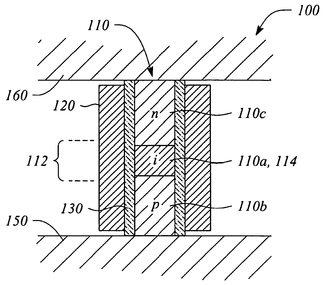
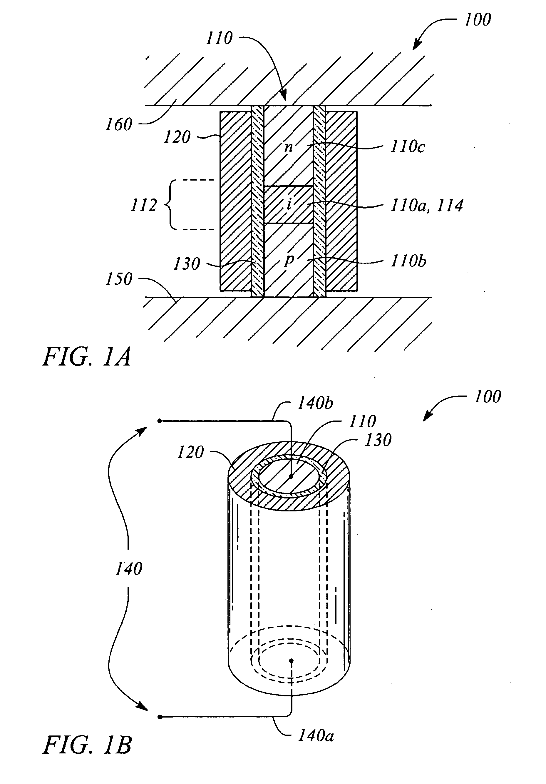
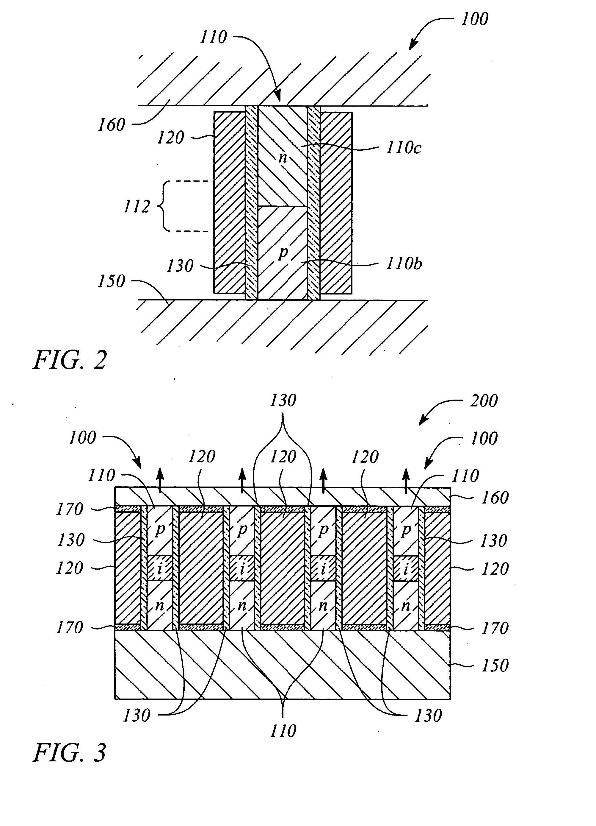
[0024]Embodiments of the present invention provide a nanowire light emitting diode (LED) with plasmonic enhancement. The plasmonic enhancement comprises plasmonic stimulation of exciton recombination through close coupling between an active region of the nanowire LED and a surface plasmon supporting layer or film. In particular, according to the embodiments of the present invention, a shell layer surrounding the nanowire comprises a material that supports surface plasmons in one or more plasmonic modes. The shell layer is coupled to the active region of a nanowire LED. The coupling between the surface plasmon and exciton recombination within the active region facilitates an increased recombination rate relative to a recombination rate without the coupling, for example. In some embodiments, the plasmonic enhancement may enhance one or both of a light emission efficiency and an effective rate of light emission or electro-optical response speed of the nanowire LED.

[0025]In particular, ...


PUM


Abstract

A nanowire light emitting diode (LED) and method of emitting light employ a plasmonic mode. The nanowire LED includes a nanowire having a semiconductor junction, a shell layer coaxially surrounding the nanowire, and an insulating layer, which is plasmonically thin, isolating the shell layer from the nanowire. The shell layer supports a surface plasmon that couples to the semiconductor junction by an evanescent field. Light is generated in a vicinity of the semiconductor junction and the surface plasmon is coupled to the semiconductor junction during light generation. The coupling enhances one or both of an efficiency of light emission and a light emission rate of the LED. A method of making the nanowire LED includes forming the nanowire, providing the insulating layer on the surface of the nanowire, and forming the shell layer on the insulating layer in the vicinity of the semiconductor junction.

Description

CROSS-REFERENCE TO RELATED APPLICATIONS[0001]The present application claims priority from provisional application Ser. No. 61 / 047668, filed Apr. 24, 2008, the contents of which are incorporated herein by reference in their entirety.STATEMENT REGARDING FEDERALLY SPONSORED RESEARCH OR DEVELOPMENT[0002]N / ABACKGROUND[0003]1. Technical Field[0004]The invention relates to light emitting diodes. In particular, the invention relates to light emitting diodes fabricated from nanostructures.[0005]2. Description of Related Art[0006]Semiconductor devices that generate or emit light are used in and often as a backbone of many modern optoelectronic or photonic systems. In particular, most modern optical communication systems depend on light emitting semiconductor devices for one or more of signal generation, signal regeneration / amplification, and signal modulation (i.e., direct modulation). Light emitting semiconductor devices are devices that generate light through carrier or exciton recombinatio...

Claims


Application Information

Patent Timeline
Patent Type & Authority Applications(United States)
IPC IPC(8): H01L33/00H01L33/18
CPCH01L33/18
Inventor CHO, HANSFATTAL, DAVIDQUITORLANDO, NATHANIEL
Owner HEWLETT-PACKARD ENTERPRISE DEV LP
Why Eureka
Try Eureka