Optoelectronic device with reflective surface

a technology of optoelectronic devices and reflective surfaces, applied in the direction of semiconductor devices, basic electric elements, electrical appliances, etc., can solve the problems of failure of the entire optoelectronic device, and achieve the effect of increasing the light emission efficiency of leds and increasing the sensitivity of light detection

Inactive Publication Date: 2005-03-08
EPISTAR CORP
View PDF3 Cites 37 Cited by
  • Summary
  • Abstract
  • Description
  • Claims
  • Application Information

AI Technical Summary

Benefits of technology

For overcoming the conventional problems described in the aforementioned background, one object of the present invention is to provide an optoelectronic device, so as to efficiently emitting light to the external from the optoelectronic device for increasing the light emission efficiency thereof, wherein the light is emitted from an optoelectronic element.
Another object of the present invention is to provide an optoelectronic device, so as to efficiently concentrate the light emitted to the optoelectronic device on a photosensitive element for increasing the sensitivity thereof (i.e. high S / N ratio).
Since the optoelectronic device of the present invention can use the reflective surface to reflect out the light emitted downwards by the LED, thereby increasing the light emission efficiency of the LED, or can reflect the light received intensively to the photosensitive element, thus increasing the sensitivity of light detection. Moreover, in the optoelectronic device of the present invention, the optoelectronic element is disposed in a space between the transparent conductive substrate and the bottom of the base, and the space does not need to be filled with any coating resin, thus preventing the optoelectronic element from being damaged by the coating resin.

Problems solved by technology

Meanwhile, since the filling material of resin currently used in packaging the element has poor resistance in general to the UV light or the light with short wavelength, it is very easy to result in the failure of the entire optoelectronic device due to the invalid filling material.

Method used


Image

  • Optoelectronic device with reflective surface
  • Optoelectronic device with reflective surface
  • Optoelectronic device with reflective surface

Examples


Embodiment Construction

Hereinafter, an optoelectronic device is explained by referring to the related figures, according to preferred embodiments of the present invention, wherein same reference numbers are used for the same elements for explanation.

According to a preferred embodiment of the present invention, an optoelectronic device comprises an optoelectronic element, a transparent conductive substrate and a base. The optoelectronic element can be an optically-active element, such as a light-emitting element, or an optically-passive element, such as a photosensitive element or a solar cell. Hereinafter, the light-emitting element in the optically-active elements will be first used as an example to explain a preferred embodiment of the present invention.

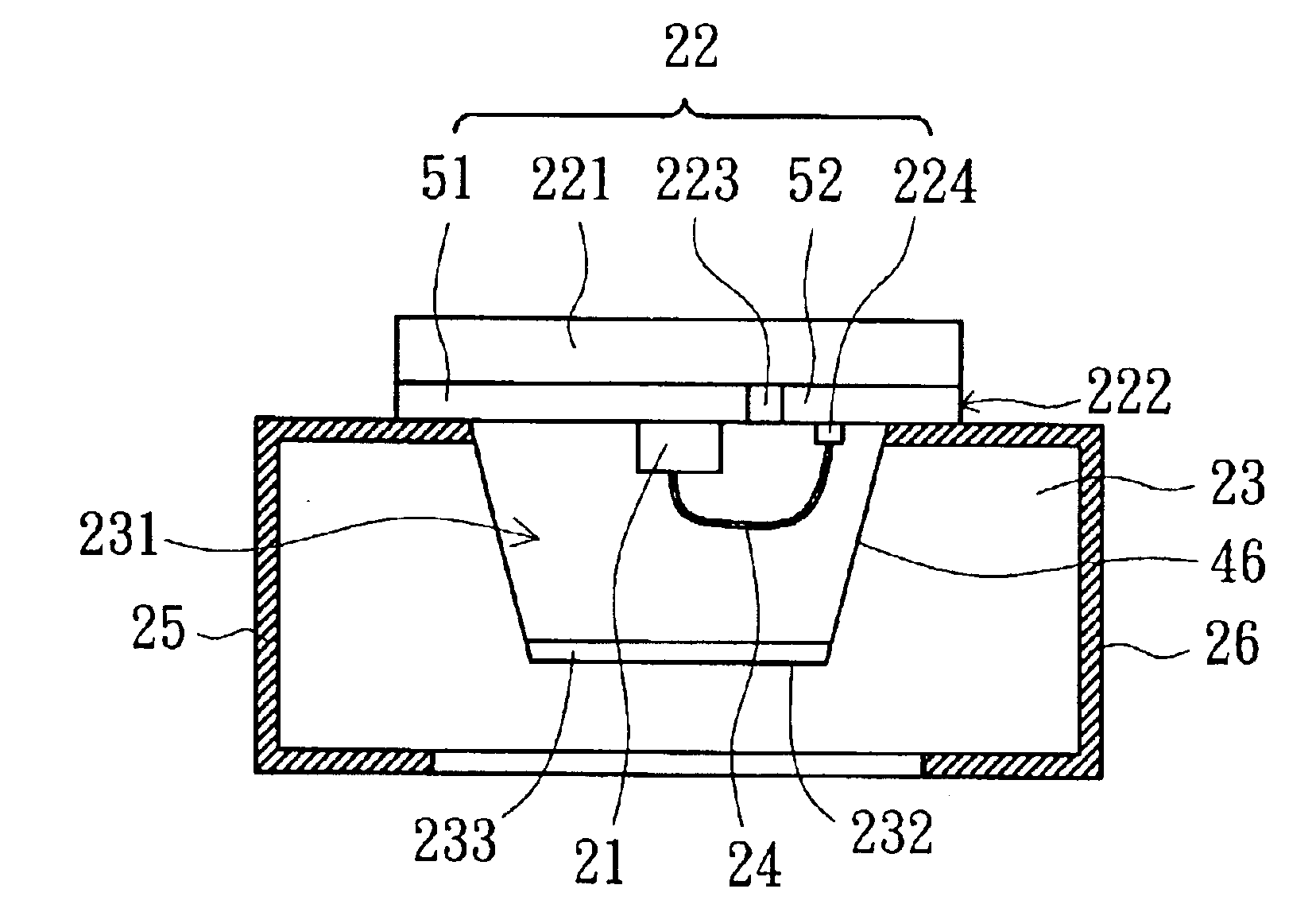
Referring to FIG. 4, the optoelectronic device shown in FIG. 4 comprises an optoelectronic element 21, a transparent conductive substrate 22, a base 23 and a conductive wire 24.

In this embodiment, the transparent conductive substrate 22 is mainly compose...


PUM


Abstract

An optoelectronic device is disclosed. The optoelectronic device comprises a transparent conductive substrate, an optoelectronic element, and a base. The transparent conductive substrate comprises a transparent plate, a transparent electrode film formed on the transparent plate, and an insulating part formed on the transparent plate. The insulating part divides the transparent electrode film into a first transparent electrode film and a second transparent electrode film that non-conduct each other. The optoelectronic element comprising a positive electrode and a negative electrode is disposed on the transparent conductive substrate and electrically connected to the first transparent electrode film and the second transparent electrode film individually. The base is formed with an opening that has a reflective surface on the bottom of the opening, and the optoelectronic element is held in the opening in a manner of suspending from or connecting with the bottom of the opening.

Description

FIELD OF THE INVENTIONThe present invention relates to an optoelectronic device, and more particularly, to an optoelectronic device that can promote light emission intensity and increasing light reception intensity.BACKGROUND OF THE INVENTIONCurrently, one of the most commonly-used optoelectronic elements is a diode, which can be roughly divided into a light-emitting element, such as a light-emitting diode (LED) and a laser diode (LD), and a photosensitive element, such as a photo-detector or a solar cell, wherein the photo-detector can be a photodiode (PD) or a positive-intrinsic-negative (PIN) diode, etc.The LED is an element having excellent optoelectronic features of low power consumption, low heat generation, long operation life, good impact resistance, small size, fast responding speed and stable emission wavelength, etc.Generally speaking, the LED can be applied to the specific purposes of various home appliances and computer equipments, such as computer peripherals, clock di...

Claims


Application Information

Patent Timeline
Patent Type & Authority Patents(United States)
IPC IPC(8): H01L33/00H01L33/48H01L33/50H01L33/60H01L33/62
CPCH01L33/486H01L33/60H01L33/62H01L33/507H01L2924/12041H01L2224/48247H01L2224/48091H01L2924/00014H01L2924/12044H01L2924/181H01L2924/00H01L2924/00012
Inventor LIN, MING-DERWANG, KWANG-RU
Owner EPISTAR CORP
Why Eureka
Try Eureka