

Semiconductor device
a technology of semiconductor devices and light emitting devices, which is applied in the direction of semiconductor devices, lasers, semiconductor lasers, etc., can solve the problems of imposing a serious impediment on the attempts to achieve light emitting with shorter wavelengths, unable to operate as a nitride semiconductor device, and becoming difficult to use in a light emitting devi
- Summary
- Abstract
- Description
- Claims
- Application Information
AI Technical Summary
Benefits of technology
Problems solved by technology
Method used
Image

Examples
example 1
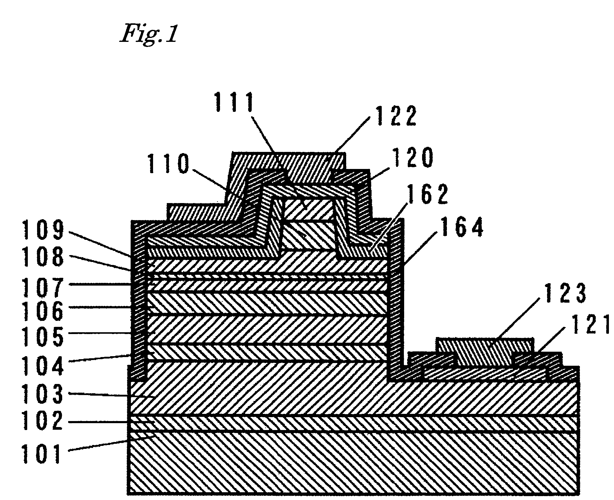
[0112]Now a laser device made of the nitride semiconductor device having the laser device structure as shown in FIG. 1 will be described below as the Example.
(Substrate 101)
[0113]For the substrate, a nitride semiconductor, GaN in this Example, is grown into a thick film (100 μm) on a substrate made of a different material. With the substrate of the different material being removed, a nitride semiconductor substrate made of GaN with a thickness of 80 μm is used. Detailed process of forming the substrate is as follows. A substrate of different material made of sapphire with the principal plane lying in the C plane having diameter of 2 inches is set in an MOVPE reaction vessel, of which temperature is set to 500° C., and a buffer layer made of GaN is formed to a thickness of 200 Å by using trimethyl gallium (TMG) and ammonia (NH3). With the temperature raised, a film of undoped GaN with thickness of 1.5 μm is grown as a base layer. Then with a plurality of striped masks formed on the b...
example 2
[0133]A laser device is obtained similarly to Example 1 except for forming the active layer as follows.
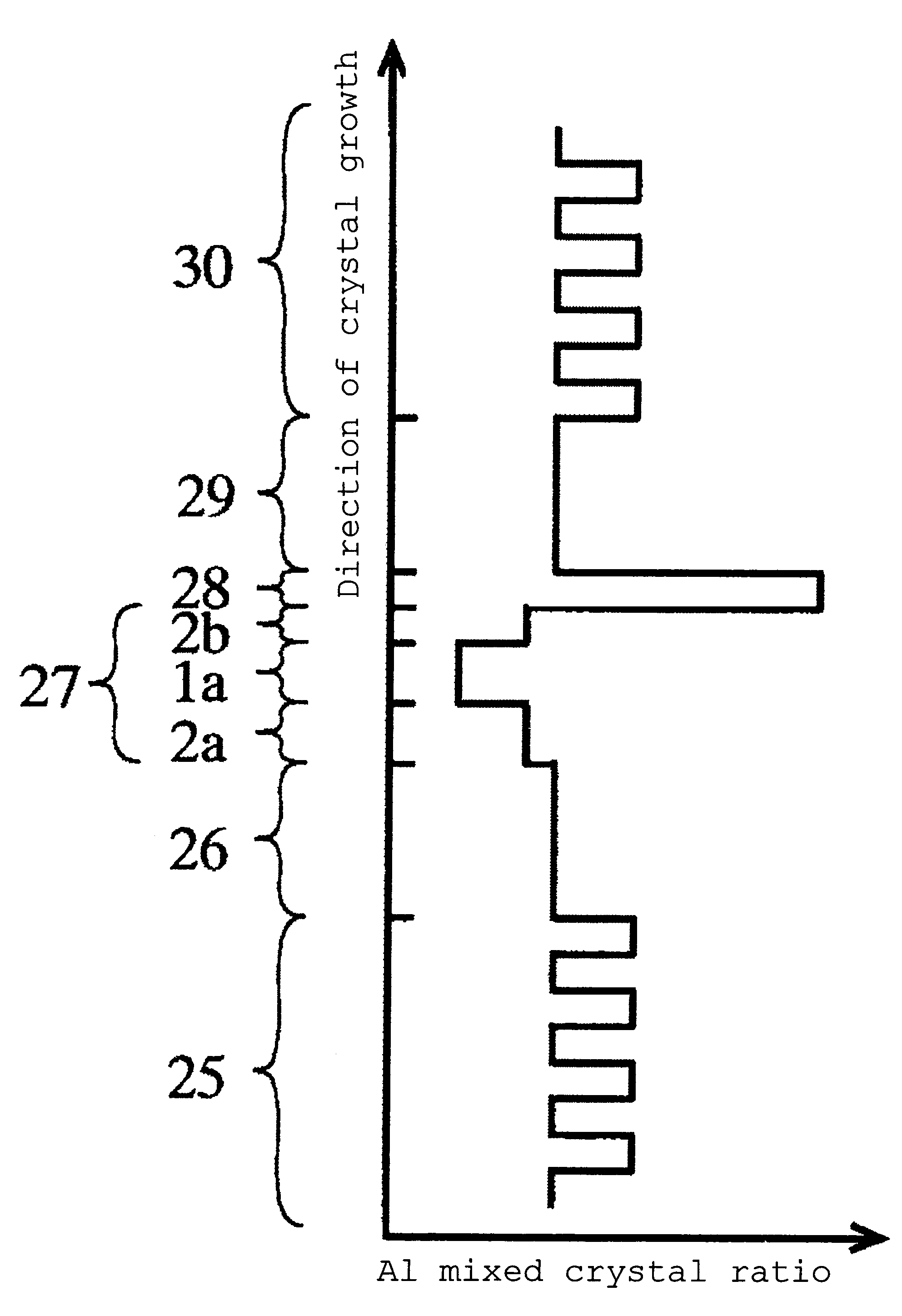
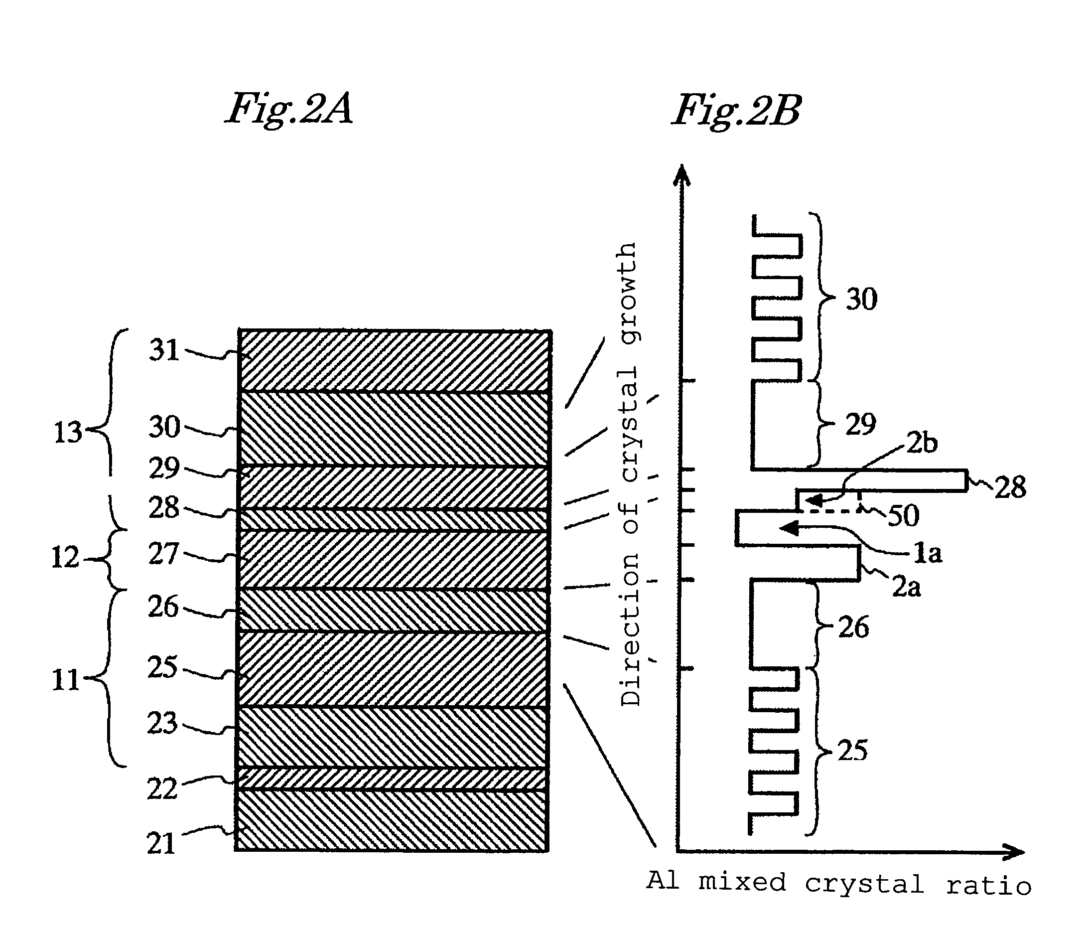
(Active Layer 107 (27, 12))
[0134]The active layer has a single quantum well structure where the first barrier layer 2a formed from Si-doped Al0.15Ga0.85N to a thickness of 150 Å, the well layer 1b formed from undoped GaN to a thickness of 100 Å and the second barrier layer 2b formed from undoped AluGa1−uN to a thickness of d (Å) stacked successively.
[0135]With the Al mixed crystal ratio u of the second barrier layer being set to 0.05 (the same Al mixed crystal ratio as in Example 1), 0.1 and 0.15 (Comparative Examples), the threshold current and device lifetime are shown in FIG. 9 and FIG. 10, respectively, as functions of the thickness of the second barrier layer. Changes in the threshold current with the changing thickness of the second barrier layer are shown in FIG. 9 with graph (a) when the Al mixed crystal ratio u of the second barrier layer is u=0.05, graph(b) when u=0.1 and...
example 3
[0139]A laser device is obtained similarly to Example 1 except for forming the active layer as follows.
(Active Layer 107 (27, 12))
[0140]The active layer has a single quantum well structure where the first barrier layer 2a formed from Si-doped Al0.15Ga0.85N to a thickness of 200 Å, the well layer 1b formed from undoped Al0.04In0.02Ga0.94N to a thickness of 100 Å and the second barrier layer 2b formed from undoped Al0.05Ga0.85N to a thickness of 150 Å stacked successively.
[0141]The laser device thus obtained, that uses quaternary compound semiconductor AlInGaN for the well layer in contrast to Example 1, oscillates continuously at an approximately the same wavelength, 370 nm, at the room temperature. Although crystallinity may not be good due to the reaction of Al and In during the crystal growth, efficiency of light emission is considered to have been improved by the inclusion of In, resulting in the threshold current of 50 mA that is lower than in the case of Example 1. Device lifet...
PUM
 Abstract
Description
Claims
Application Information