Light-emitting diode

Inactive Publication Date: 2012-05-10
PANASONIC CORP
View PDF2 Cites 41 Cited by
  • Summary
  • Abstract
  • Description
  • Claims
  • Application Information

AI Technical Summary

Benefits of technology

[0035]According to the present disclosure, a through hole is provided in the first semiconductor layer whose principal surface is an m-plane, whereby a plane whose contact resistance relative to a conductor portion is lower than that of the m-plane, for example, +c-plane or a-plane, can appear on the inner wall of the through hole. By bringing the conductor portion which is part of an electrode into contact with the inner wall of the through hole, the total contact resistance between the first semiconductor layer of the first conductivity type and the electrodes can be decreased. As a result, the voltage applied to the active layer can be maintained to a sufficient magnitude, and the power efficiency can be improved. Also, the probability of heat emission which is attributed to the contact resistance decreases.
[0036]Furthermore, release of heat from the chip is enhanced by the condu

Problems solved by technology

This effect reduces the probability of radiative recombination of carriers in t

Method used


Image

  • Light-emitting diode
  • Light-emitting diode
  • Light-emitting diode

Examples


Example

Embodiment 1

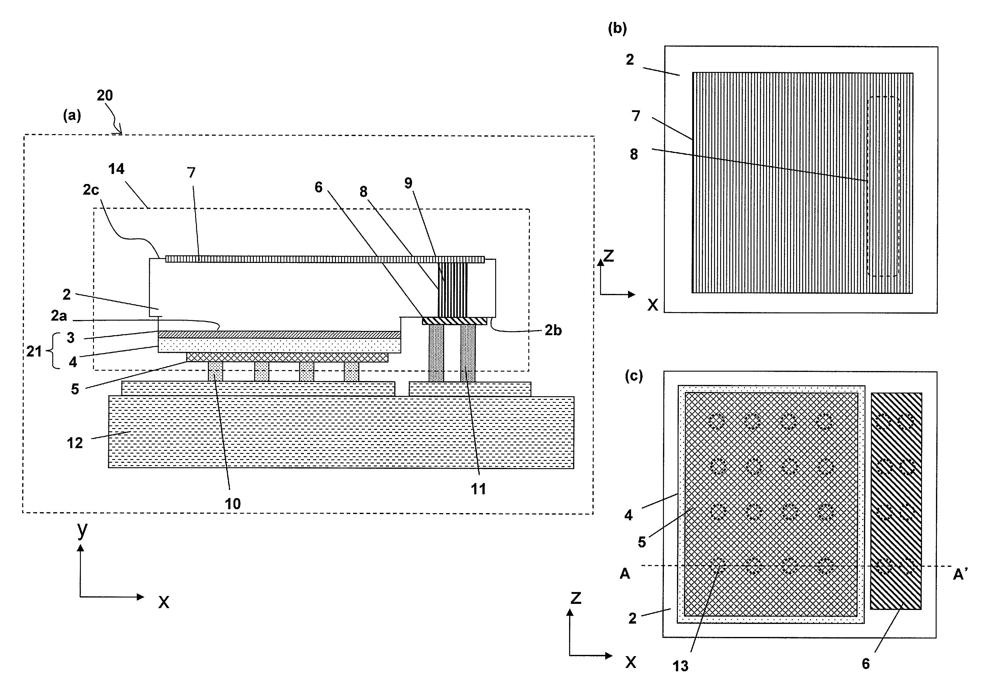
[0060]FIG. 6(a) is a cross-sectional view showing Embodiment 1 of the light-emitting diode device according to the present invention. FIG. 6(b) is a diagram showing a rear surface 1b of an n-type GaN substrate 1 of a light-emitting diode element 14. FIG. 6(c) is a diagram showing a surface of the light-emitting diode element 14 on the principal surface side. In FIGS. 6(a) to 6(c), components which are the same as those of FIG. 4(a) to FIG. 4(c), FIG. 5(a), and FIG. 5(b) are denoted by the same marks.

[0061]As shown in FIG. 6(a), a light-emitting diode device 20 of the present embodiment has a configuration wherein a light-emitting diode element (chip) 14 is mounted on the mounting base 12. The light-emitting diode element 14 is provided on the mounting base 12 via bumps 10, 11. The bump 10 couples a p-electrode 5 of the light-emitting diode element 14 with the mounting base 12. The bump 11 couples an n-type front surface electrode 6 of the light-emitting diode element 14 ...

Example

Embodiment 2

[0089]FIG. 9(a) is a cross-sectional view showing Embodiment 2 of the light-emitting diode device according to the present invention. FIG. 9(b) is a diagram showing a rear surface 1b of an n-type GaN substrate 1 shown in FIG. 9(a). FIG. 9(c) is a diagram showing a surface of a light-emitting diode element 14 shown in FIG. 9(a) which is on the principal surface side. In FIGS. 9(a) to 9(c), components which are the same as those of FIGS. 6(a) to 6(c) are denoted by the same marks.

[0090]As shown in FIG. 9(a), in the present embodiment, the +c-plane 8a and the −c-plane 8b appear on the lateral surfaces of the inner walls of the through hole 8. The +c-plane 8a is located at a position closer to the active layer 3 than the −c-plane 8b. As described above, after the heat treatment, the +c-plane exhibits low contact resistance, which is 1 / 10 to about ⅕ of the contact resistance obtained in the case of the m-plane. In this way, the +c-plane is provided on a side where a larger el...

Example

Embodiment 3

[0096]FIG. 11(a) is a cross-sectional view showing Embodiment 3 of the light-emitting diode device according to the present invention. FIG. 11(b) is a diagram showing a rear surface 1b of an n-type GaN substrate 1 shown in FIG. 11(a). FIG. 11(c) is a diagram showing a surface of a light-emitting diode element 14 shown in FIG. 11(a) which is on the principal surface side. In FIGS. 11(a) to 11(c), components which are the same as those of FIGS. 6(a) to 6(c) are denoted by the same marks.

[0097]As shown in FIGS. 11(a) to 11(c), in the present embodiment, through holes 8 are provided in a central portion of the chip (a central portion in terms of the x direction). At opposite sides of a region in which the through holes 8 are provided (the opposite sides of the chip in terms of the x direction), the active layer 3 and the p-type conductive layer 4 are positioned. As shown in FIG. 11(b), three through holes 8 are aligned along the z direction. The upper openings of the three t...


PUM


Abstract

A light-emitting diode element includes: an n-type conductive layer 2 being made of a gallium nitride-based compound, a principal surface being an m-plane; a semiconductor multilayer structure 21 provided on a first region 2a of the principal surface of the n-type conductive layer 2, the semiconductor multilayer structure 21 including a p-type conductive layer 4 and an active layer 3; a p-electrode 5 provided on the p-type conductive layer 4; a conductor portion 9 provided on a second region 2b of the principal surface of the n-type conductive layer 2, the conductor portion 9 being in contact with an inner wall of a through hole 8; and an n-type front surface electrode 6 provided on the second region 2b of the principal surface of the n-type conductive layer 2, the n-type front surface electrode 6 being in contact with the conductor portion 9.

Description

[0001]This is a continuation of International Application No. PCT / JP2010 / 004509, with an international filing date of Jul. 12, 2010, which claims priority of Japanese Patent Application No. 2009-171499, filed on Jul. 22, 2009, the contents of which are hereby incorporated by reference.TECHNICAL FIELD[0002]The present disclosure relates to a light-emitting diode and particularly to a non-polar plane light-emitting diode.BACKGROUND ART[0003]A nitride semiconductor including nitrogen (N) as a Group V element is a prime candidate for a material to make a short-wave light-emitting device because its bandgap is sufficiently wide. Among other things, gallium nitride-based compound semiconductors (which will be referred to herein as “GaN-based semiconductors”) have been researched and developed particularly extensively. As a result, blue light-emitting diodes (LEDs), green LEDs, and semiconductor laser diodes made of GaN-based semiconductors have already been used in actual products (See, f...

Claims


Application Information

Patent Timeline
IPC IPC(8): F21V21/00H01L33/38
CPCH01L33/382H01L33/16H01L33/32
Inventor IWANAGA, JUNKOYOKOGAWA, TOSHIYAYAMADA, ATSUSHI
Owner PANASONIC CORP
Why Eureka
Try Eureka