Electromagnetic wave detector and electromagnetic wave detector array

a detector array and electromagnetic wave technology, applied in the field electromagnetic wave detector arrays, can solve the problems of inability to effectively acquire optical information as electromagnetic wave detectors, inability to use the optimum semiconductor of electromagnetic wave detectors, and inability to achieve the function of detecting the polarization of incident light in conventional electromagnetic wave detectors using graphene, etc., to achieve high-sensitivity photodetection and increase the effect of optical absorption ra

Active Publication Date: 2014-10-30
MITSUBISHI ELECTRIC CORP
View PDF3 Cites 56 Cited by
  • Summary
  • Abstract
  • Description
  • Claims
  • Application Information

AI Technical Summary

Benefits of technology

[0010]By using the electromagnetic wave detector according to the present invention, by isolated metals-graphene-an intermediate layer-a metal layer, or by graphene-isolated metals-an intermediate layer-a metal layer, there is formed a cavity in which a specific surface plasmon mode ...

Problems solved by technology

However, because the semiconductor material has a band gap, only light having larger energy than the band gap can be detected, and therefore, the semiconductor cannot be said to be optimum for an electromagnetic wave detector.
However, because a photoabsorbing layer formed of only graphene has ...

Method used


Image

  • Electromagnetic wave detector and electromagnetic wave detector array
  • Electromagnetic wave detector and electromagnetic wave detector array
  • Electromagnetic wave detector and electromagnetic wave detector array

Examples


embodiment 1

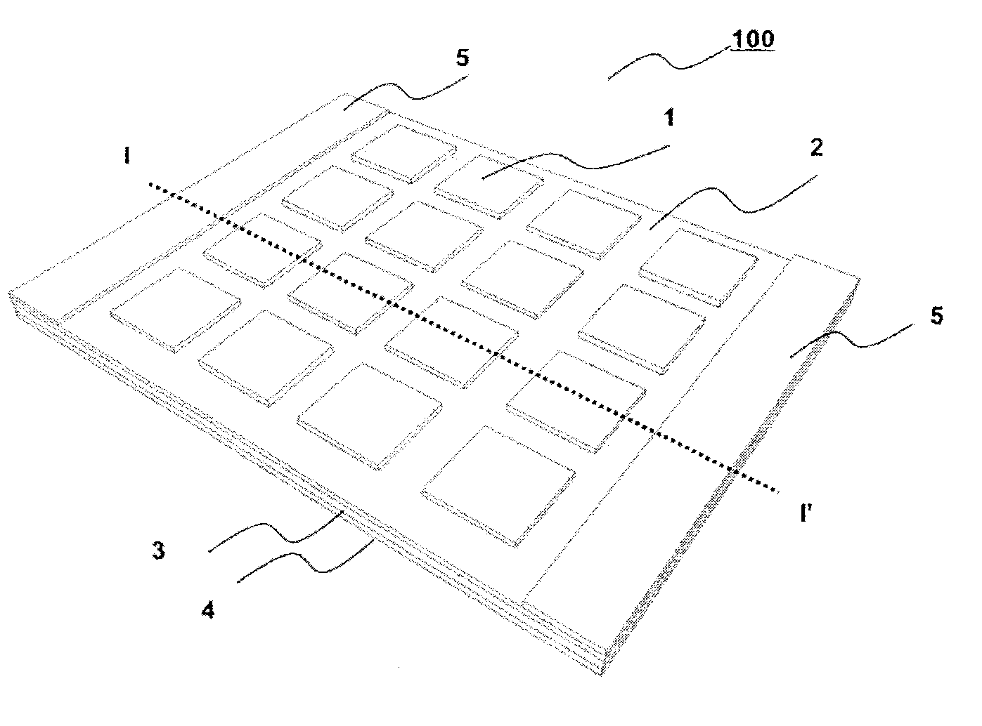
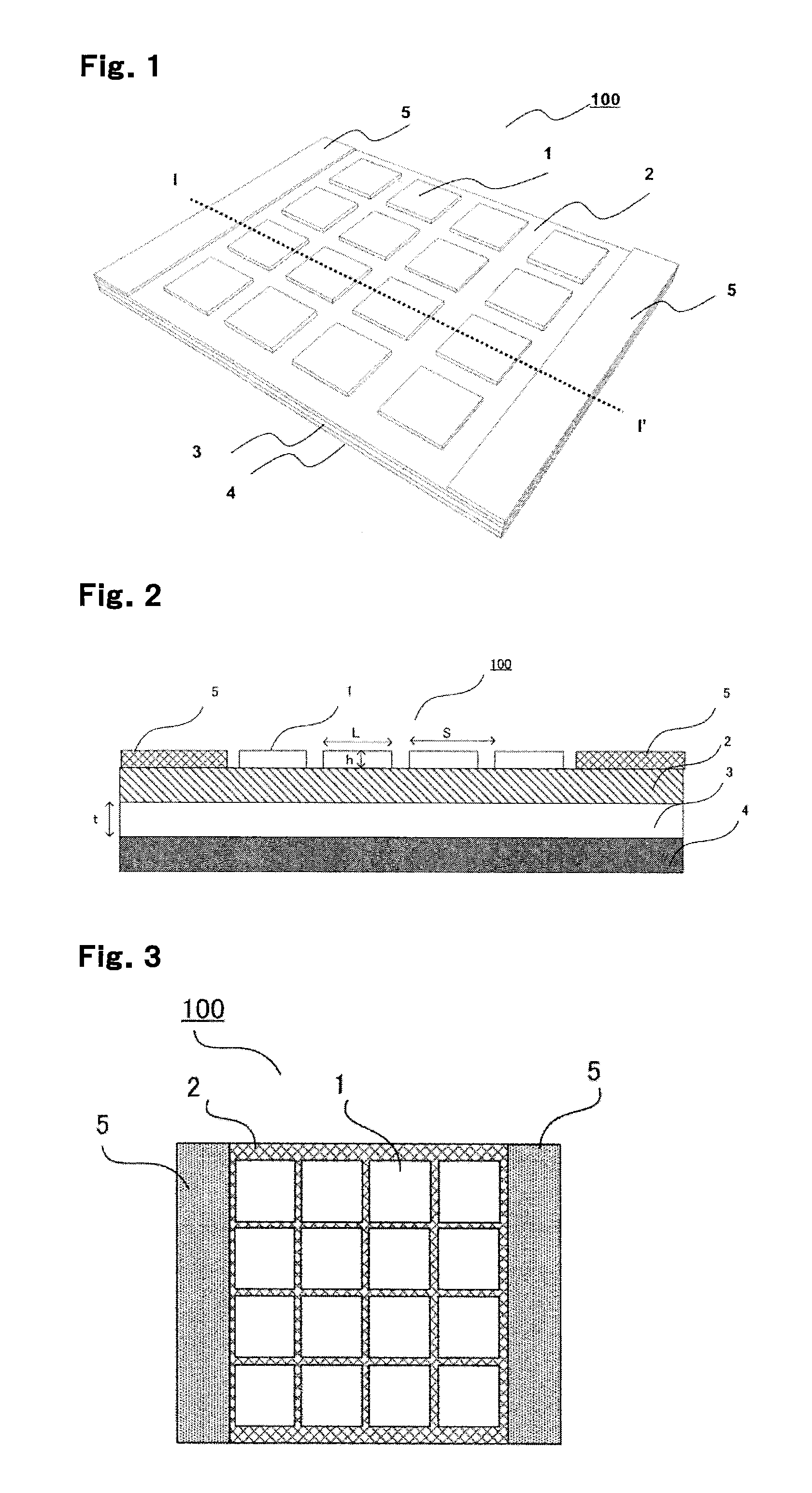
[0104]FIG. 1 is a perspective view of an electromagnetic wave detector according to Embodiment 1 of the present invention, the whole electromagnetic wave detector being denoted by 100. FIG. 2 is a sectional view of the electromagnetic wave detector taken along I-I′ in FIG. 1. FIG. 3 is a top view of the electromagnetic wave detector in FIG. 2 when viewed from an upper surface (also referred to as a “surface” or an “incident surface”).

[0105]As shown in FIGS. 1 to 3, and particularly, in FIG. 2, in the electromagnetic wave detector 100, a metal layer 4 is formed on a substrate (not shown), an insulating layer 3 having a thickness t is provided on an upper surface of the metal layer 4, and a graphene layer 2 is provided on an upper surface of the insulating layer 3. On the graphene layer 2, isolated metals 1 are arranged in a matrix form, each isolated metal 1 in a square shape having a length L in one side and a thickness h, so that periods of the isolated metals 1 in two orthogonal d...

embodiment 2

[0154]FIG. 13A is a perspective view of an electromagnetic wave detector 110 according to Embodiment 2 of the present invention. The electromagnetic wave detector 110 is different from the electromagnetic wave detector 100 according to Embodiment 1 in that the graphene layer 2 is not arranged in a sheet shape, but the graphene layer 2 is partly processed to be used as a graphene connection wiring 6. That is, the graphene layer 2 is provided in only lower parts of the isolated metals 1 and the electrodes 5, and in portions of the graphene connection wirings 6 that connect the isolated metals 1 and the electrodes 5.

[0155]The electromagnetic wave detector 110 shown in FIG. 13A can be obtained by forming the isolated metals 1, and then removing a part of the graphene layer 2 by a photoengraving step, for example. FIG. 13B is a conceptual view about the electric resistance value that is observed between two electrodes 5, in the electromagnetic wave detector 100 according to Embodiment 1....

embodiment 3

[0164]FIG. 15 is a perspective view of an electromagnetic wave detector according to Embodiment 3 of the present invention, the whole electromagnetic wave detector being denoted by 140. In the electromagnetic wave detector 140, the isolated metals 1 are connected in series by the graphene connection wiring 6 between two electrodes 5. In the electromagnetic wave detector 140 shown in FIG. 15, when a resistance value of the graphene layer 2 arranged below the isolated metals 1 is denoted by R1 and a resistance value of the graphene connection wiring 6 between the isolated metal 1 and the isolated metal 1 is denoted by R2, a resistance value R between the electrodes 5 when n isolated metals 1 are connected in series can be expressed as follows.

R=n×R1+n×R2

Therefore, the following relation is obtained.

RW=nR1W

[0165]That is, in the electromagnetic wave detector 140 shown in FIG. 15, stronger electric signal intensity for the light intensity of a specific wavelength can be obtained, and the...


PUM


Abstract

An electromagnetic wave detector that detects incident light by converting the incident light into an electric signal includes a flat metal layer formed on a supporting substrate, an intermediate layer formed on the metal layer, a graphene layer formed on the intermediate layer, isolated metals periodically formed on the graphene layer, and electrodes arranged oppositely on both sides of the isolated metals. Depending on a size of a planar shape of each of the isolated metals, light having a predetermined wavelength at which surface plasmon occurs is determined out of the incident light, and the light having the predetermined wavelength is absorbed to detect a change in the electric signal generated in the graphene layer.

Description

BACKGROUND OF THE INVENTION[0001]1. Field of the Invention[0002]The present invention relates to an electromagnetic wave detector and an electromagnetic wave detector array, and more particularly to an electromagnetic wave detector and an electromagnetic wave detector array using single or multilayer graphene as a photodetecting layer.[0003]2. Description of Related Art[0004]In conventional electromagnetic wave detectors, semiconductor materials are used for photodetecting layers. However, because the semiconductor material has a band gap, only light having larger energy than the band gap can be detected, and therefore, the semiconductor cannot be said to be optimum for an electromagnetic wave detector. Therefore, attention has been focused on graphene as a next-generation light detection material. Graphene is a monoatomic layer of a two-dimensional carbon crystal, and single-layer graphene has a very small thickness of 0.34 nm which is equivalent to one carbon atom. Graphene has a ...

Claims


Application Information

Patent Timeline
IPC IPC(8): G01J1/42
CPCG01J1/42G01J1/0429G01J5/046G01J5/0881G01J1/04G01J5/20G02B5/008G01J5/0853G02B5/1809H01L31/09H01L31/108H01L2031/0344G01J1/0204G01J5/59H01L27/12H01L31/1085
Inventor OGAWA, SHIMPEIFUJISAWA, DAISUKEMAEGAWA, TOMOHIRO
Owner MITSUBISHI ELECTRIC CORP
Why Eureka
Try Eureka