Phase Change Memory Device and Manufacturing Method

a memory device and phase change technology, applied in semiconductor devices, digital storage, instruments, etc., can solve problems such as problems in manufacturing such devices with very small dimensions

Active Publication Date: 2007-05-31
MACRONIX INT CO LTD
View PDF86 Cites 215 Cited by
  • Summary
  • Abstract
  • Description
  • Claims
  • Application Information

AI Technical Summary

Benefits of technology

[0011] A first aspect of the invention is directed to a phase change memory device comprising a memory cell access layer and a memory cell layer, operably coupled to the memory cell access layer, comprising a photolithographically formed phase change memory cell. The memory cell comprises first and second electrodes, having first and second opposed, spaced apart sides, and a phase change bridge positioned between the first and second sides and electrically coupling the first and second sides to one anothe

Problems solved by technology

Problems have arisen in manufacturing such devices with very small dimensions, and with v

Method used


Image

  • Phase Change Memory Device and Manufacturing Method
  • Phase Change Memory Device and Manufacturing Method
  • Phase Change Memory Device and Manufacturing Method

Examples


Embodiment Construction

[0029] The following description of the invention will typically be with reference to specific structural embodiments and methods. It is to be understood that there is no intention to limit the invention to the specifically disclosed embodiments but that the invention may be practiced using other features, elements, methods and embodiments. Like elements in various embodiments are commonly referred to with like reference numerals.

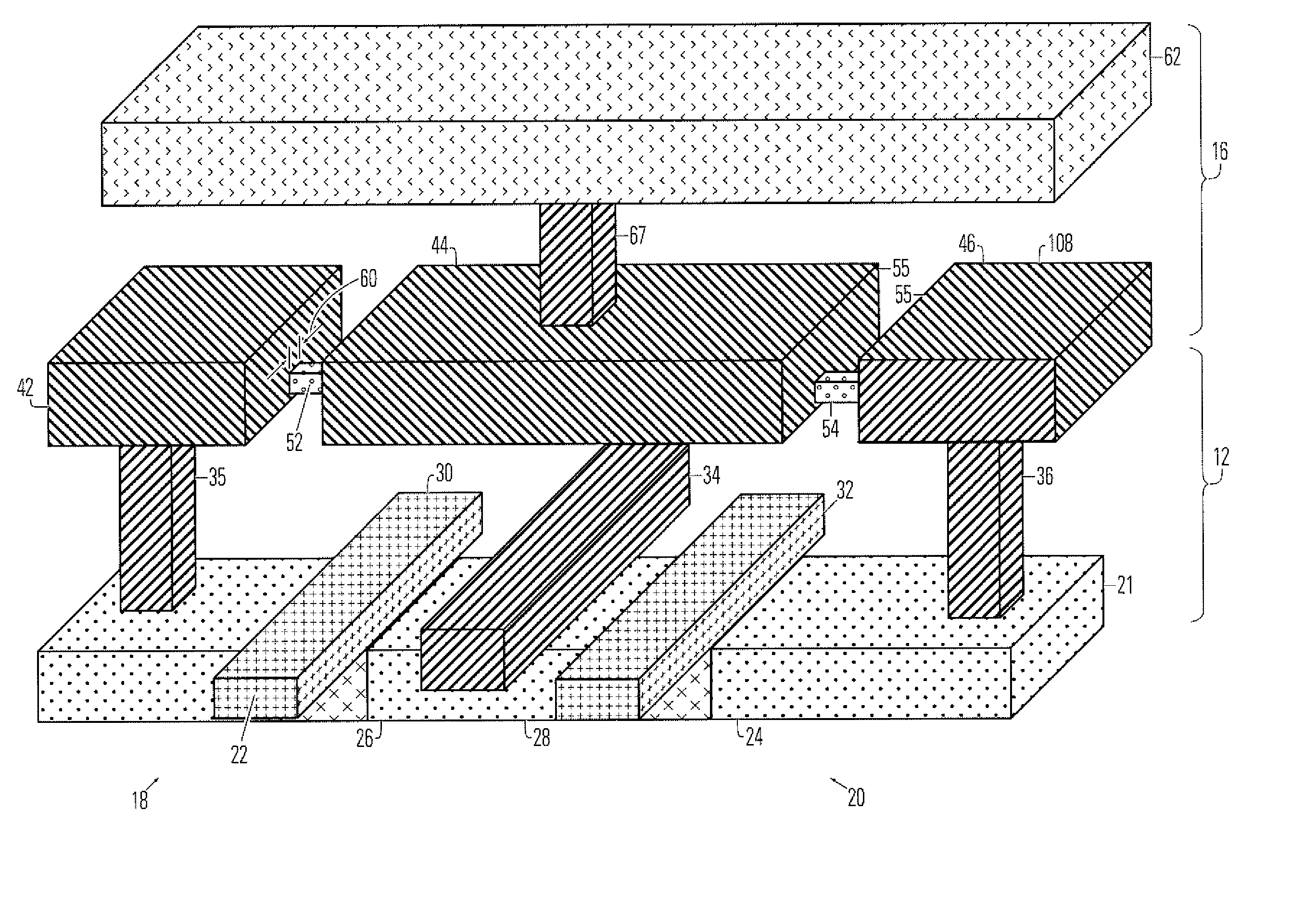
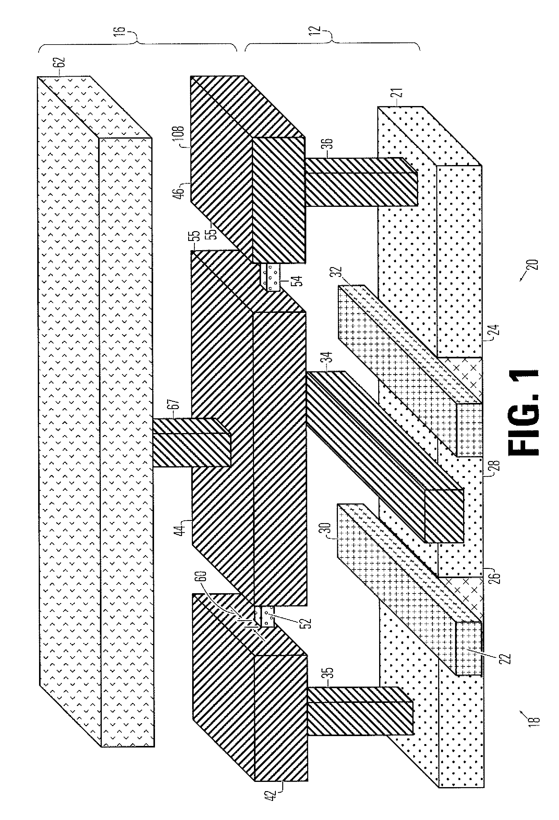
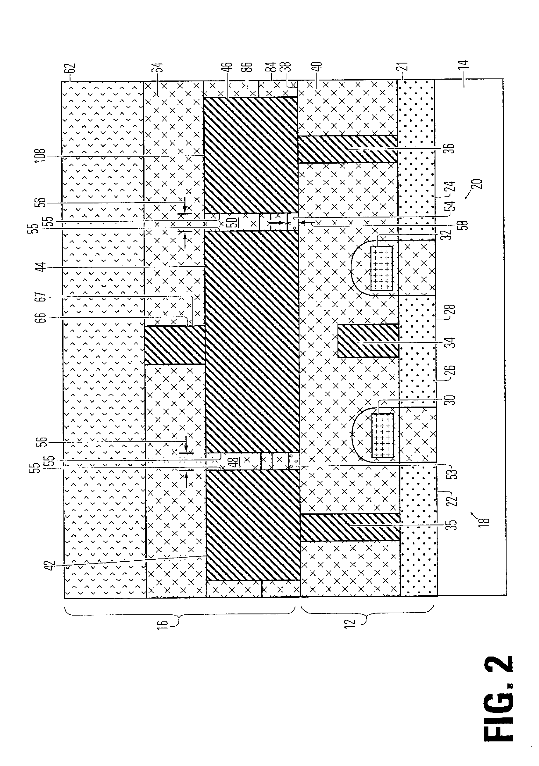
[0030]FIGS. 1 and 2 are two views of a phase change memory device 10 made according to one embodiment of the invention. Device 10 comprises broadly a memory cell access layer 12 formed on a substrate 14 and a memory cell layer 16 formed on top of access layer 12. In this embodiment, access layer 12 comprises first and second access transistors 18, 20 formed at doped layer 21. Access transistors 18, 20 comprise first and second drains 22, 24, first and second sources 26, 28, first and second polysilicon word lines acting as first and second gates 30, 32, an...


PUM


Abstract

A phase change memory device comprises a photolithographically formed phase change memory cell having first and second electrodes and a phase change bridge positioned between and electrically coupling the opposed sides of the electrodes to one another. The phase change bridge has a length, a width and a thickness. The width, the thickness and the length are less than a minimum photolithographic feature size of the process used to form the phase change memory cell. The size of the photoresist masks used in forming the memory cell may be reduced so that the width and the length of the phase change bridge are each less than the minimum photolithographic feature size.

Description

CROSS REFERENCE TO RELATED APPLICATIONS [0001] This application claims the benefit of provisional patent application No. 60 / 736,722 filed 15 Nov. 2005, Attorney Docket number MXIC 1620-1.PARTIES TO A JOINT RESEARCH AGREEMENT [0002] International Business Machines Corporation, a New York corporation; Macronix International Corporation, Ltd., a Taiwan corporation, and Infineon Technologies A.G., a German corporation, are parties to a Joint Research Agreement. BACKGROUND OF THE INVENTION [0003] 1. Field of the Invention [0004] The present invention relates to high density memory devices based on phase change based memory materials, including chalcogenide based materials and other materials, and to methods for manufacturing such devices. [0005] 2. Description of Related Art [0006] Phase change based memory materials are widely used in read-write optical disks. These materials have at least two solid phases, including for example a generally amorphous solid phase and a generally crystall...

Claims


Application Information

Patent Timeline
IPC IPC(8): G11C11/00
CPCG11C13/0004G11C2213/79H01L27/2436H01L45/06H01L45/1226H01L45/144H01L45/1675H01L45/1691H10B63/30H10N70/823H10N70/231H10N70/068H10N70/8828H10N70/063
Inventor LUNG, HSIANG LANCHEN, SHIH-HUNG
Owner MACRONIX INT CO LTD
Why Eureka
Try Eureka