Display device

a display device and display technology, applied in the field of display devices, can solve the problems of increased cost and degraded display quality, and achieve the effects of reducing the likelihood of flashing, and preventing direct current applications

Inactive Publication Date: 2007-06-28
HITACHI DISPLAYS
View PDF6 Cites 18 Cited by
  • Summary
  • Abstract
  • Description
  • Claims
  • Application Information

AI Technical Summary

Benefits of technology

[0014] An object of the invention is to provide a technology capable of reducing an afterimage in an inexpensive manner when a hold response display is used in an I / P conversion display mode.
[0020] In the display device of the invention, as described with reference to the device of (1), when the pixel electrode connected to the source electrode of the TFT element repeatedly receives the signal of positive polarity and the signal of negative polarity same even number of times for each signal, the occurrence of the signal of positive or negative polarity is periodically changed to an odd number. In this way, the phase of the voltage of the signal applied to the pixel electrode before the occurrence of the signal is changed to the odd number differs from that after the change, thereby preventing direct current application and hence reducing an afterimage in the I / P conversion display mode.
[0022] To prevent the direct current application and reduce the likelihood of flashing, for example, it is preferable to provide the device described in (3). In this case, for example, by periodically applying a signal of either polarity in succession to the TFT elements connected to two gate electrode lines at a time, the phases of the signals for the TFT elements connected to the two gate electrode lines can be changed at a time, thereby preventing the direct current application. Also, application of a signal of same polarity in succession, which causes flashing, is carried out for two lines at a time, so that flashing becomes less noticeable compared to the case where all the phases of the signals are changed at once.
[0023] By providing the devices described in (1) to (3), the direct current application can be prevented and the flashing can be reduced by changing the polarities in data, so that an expensive frame memory is not required and there occurs no increase in cost.

Problems solved by technology

However, it has been newly found that when the I / P conversion is used to display images, for example, an afterimage disadvantageously occurs at the boundary between two areas that greatly differ in gray scale level of display data, resulting in significantly degraded display quality.
This method, however, disadvantageously requires at least a frame memory corresponding to the size of the screen, resulting in increased cost.

Method used


Image

  • Display device
  • Display device
  • Display device

Examples


Embodiment Construction

[0037] The invention will be described below in detail along with embodiments (examples) thereof with reference to the drawings. Throughout the drawings for explaining the examples, those having same functions have same reference characters and redundant description thereof will be omitted.

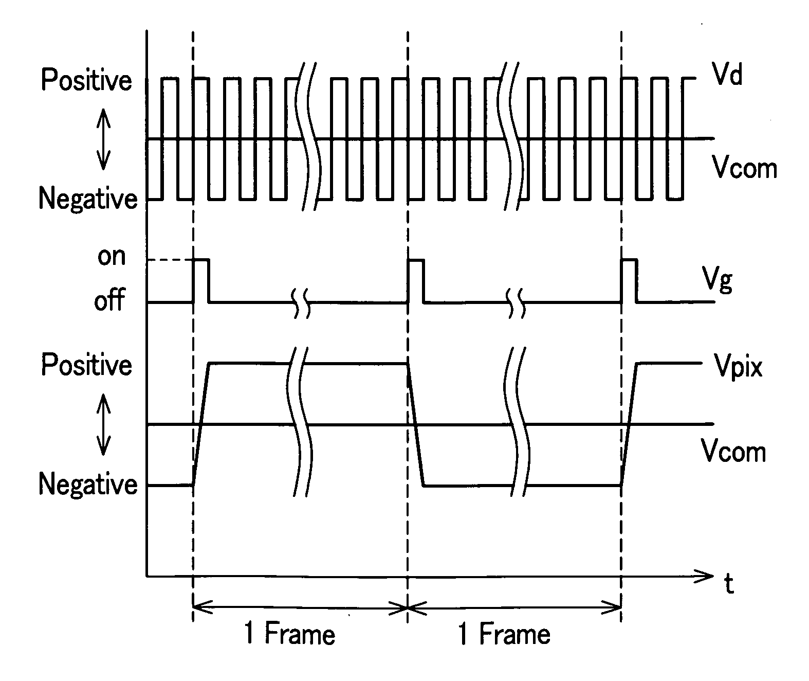
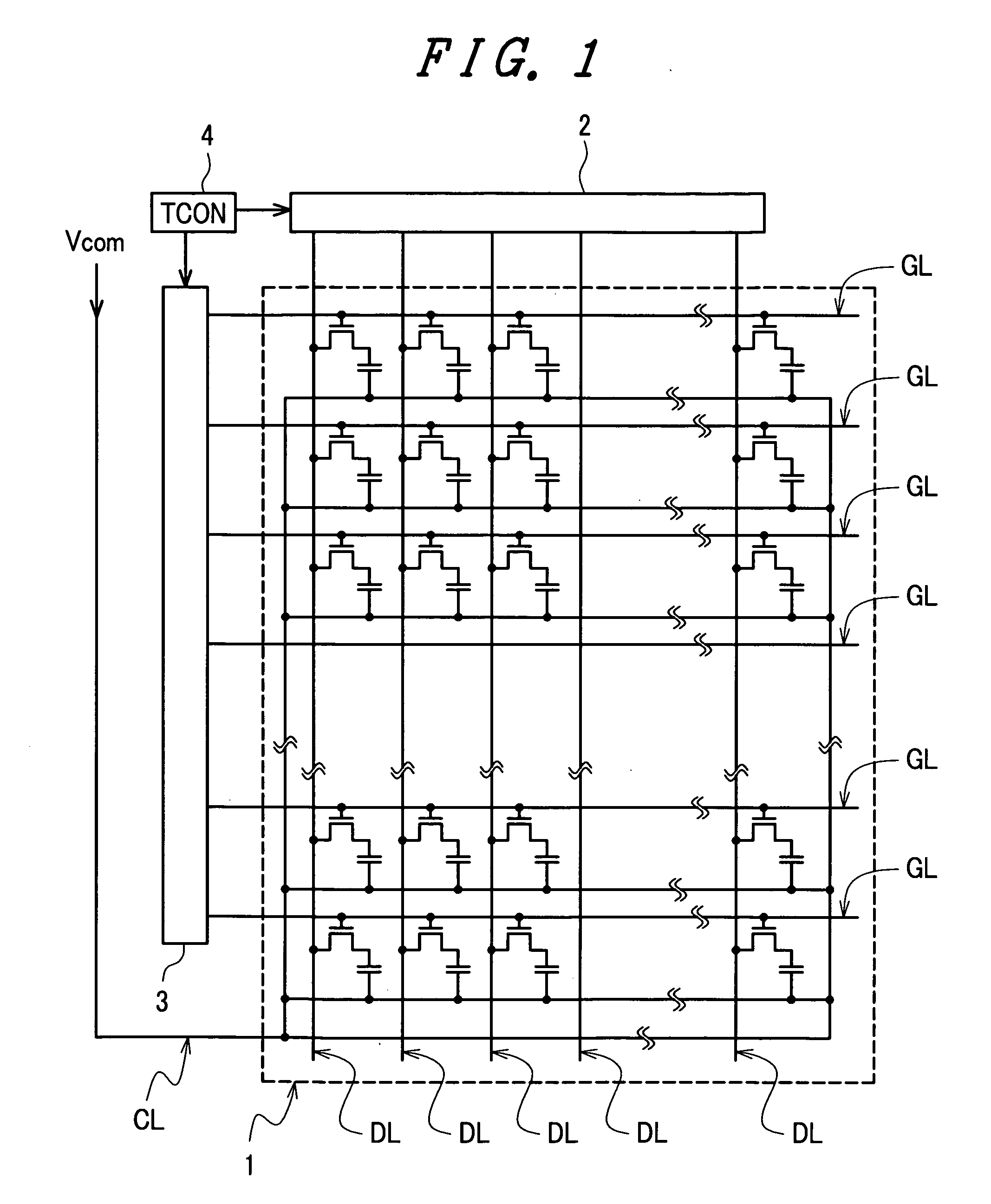
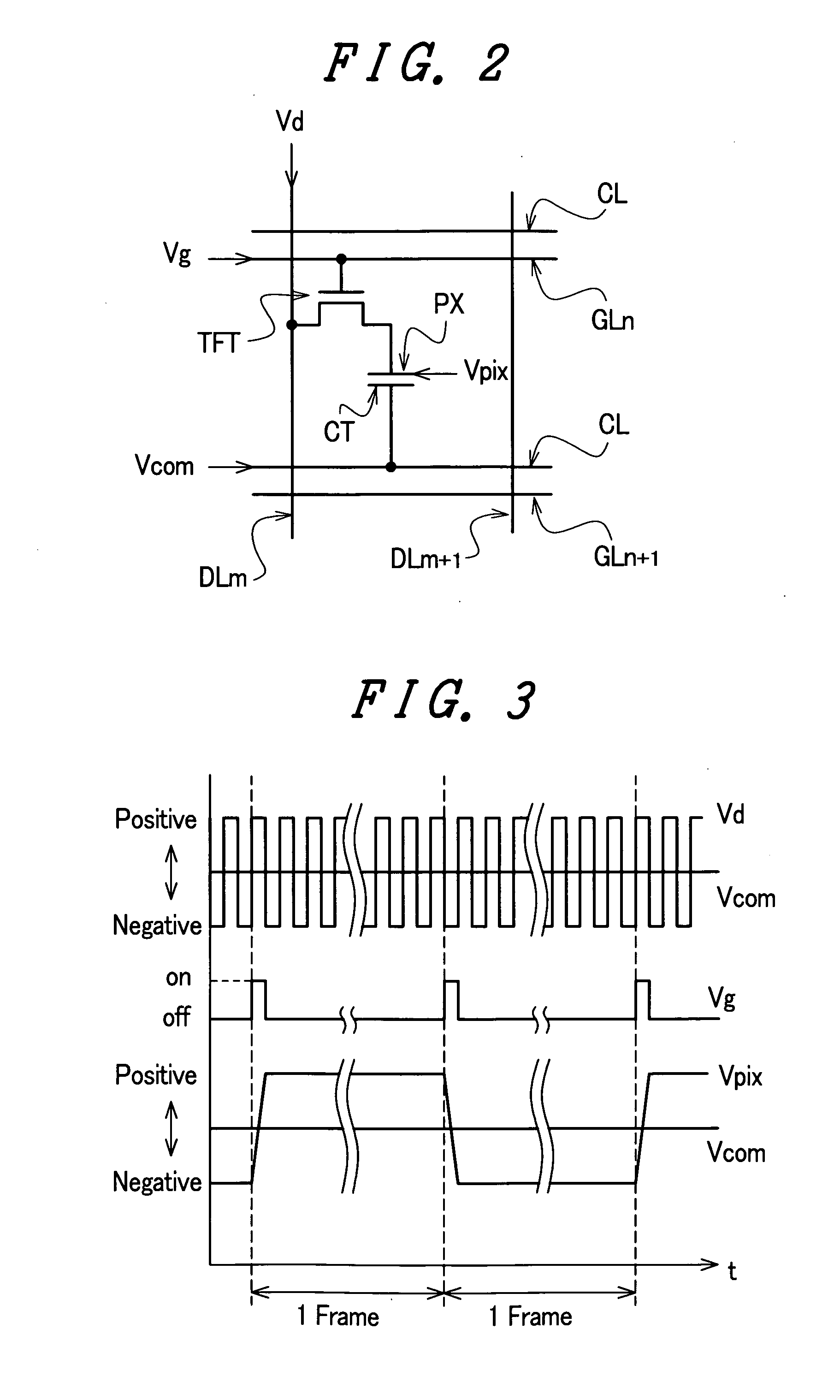
[0038]FIGS. 1 and 2 are diagrammatic views showing one example of a circuit configuration of a display device to which the invention is applied. FIG. 1 shows an overall circuit configuration and FIG. 2 shows a circuit configuration of one pixel.

[0039] The display device to which the invention is applied has a plurality of drain electrode lines DL and a plurality of gate electrode lines GL arranged in a matrix in a display area 1, for example as shown in FIG. 1. The drain electrode lines DL are connected to a data driver 2, while the gate electrode lines GL are connected to a scan driver 3. The area surrounded by two adjacent drain electrode lines DL and two adjacent gate electrode lines GL is a ...


PUM


Abstract

An afterimage produced when a hold response display is used in an I / P conversion display mode is reduced. This is achieved by a display device comprising: a plurality of drain electrode lines and a plurality of gate electrode lines arranged in a matrix; and pixel areas, each surrounded by two adjacent ones of the drain electrode lines and two adjacent ones of the gate electrode lines, each pixel area having a TFT element, the assembly of the pixel areas defining a display area, wherein a drain electrode of the TFT element is electrically connected to the drain electrode line, a source electrode of the TFT element is electrically connected to a pixel electrode, the pixel electrode repeatedly receives a signal of positive polarity even or odd number of times and a signal of negative polarity the same number of times as the signal of positive polarity, and one or both of the occurrence of the signal of negative polarity and the signal of positive polarity are periodically changed to an odd number when the occurrence of the signal of positive polarity is an even number, or to an even number when the occurrence of the signal of positive polarity is an odd number.

Description

CLAIM OF PRIORITY [0001] The present application claims priority from Japanese application serial No. 20005-279186, filed on (Sep. 27, 2005), the content of which is hereby incorporated by reference into this application. BACKGROUND OF THE INVENTION [0002] 1. Field of the Invention [0003] The present invention relates to a display device, and particularly to a technology that is effective when applied to a hold-type display device with TFT (thin film transistor) elements arranged in a matrix on a pixel basis. [0004] 2. Description of the Related Art [0005] Conventionally, a display is roughly divided into an impulse response display and a hold response display, when classified in terms of displaying motion image. The impulse response display is characterized in that the brightness responds such that it decreases immediately after the scan, for example, as with afterglow characteristics of a cathode ray tube. The hold response display is characterized in that the brightness based on ...

Claims


Application Information

Patent Timeline
Patent Type & Authority Applications(United States)
IPC IPC(8): G09G3/36
CPCG09G3/3614G09G2310/0229G09G2320/0204G09G2320/0247G09G2320/0257
Inventor OKE, RYUTAROIMAJO, YOSHIHIRO
Owner HITACHI DISPLAYS
Why Eureka
Try Eureka