Wafer-level chip package process

Active Publication Date: 2007-07-05
ADVANCED SEMICON ENG INC
View PDF5 Cites 9 Cited by
  • Summary
  • Abstract
  • Description
  • Claims
  • Application Information

AI Technical Summary

Benefits of technology

[0010]Accordingly, the present invention is directed to provide a wafer-lev

Problems solved by technology

Thus, during the procedure of cutting the back surface of the wafer to form the second groove, water vapor may seep into the chamb

Method used


Image

  • Wafer-level chip package process
  • Wafer-level chip package process
  • Wafer-level chip package process

Examples


Example

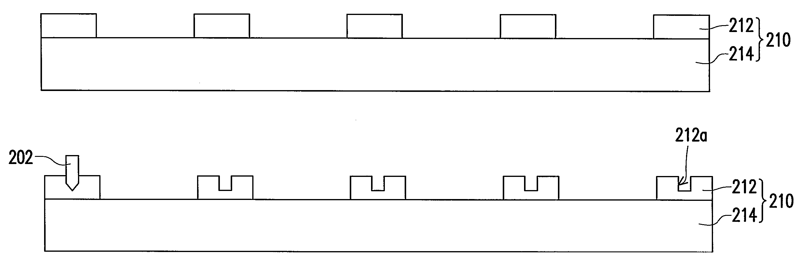
[0024]FIGS. 2A˜2G are flowcharts illustrating a wafer-level chip package process according to an exemplary embodiment of the present invention. In the present embodiment, the wafer-level chip package process includes the following steps. First, as shown in FIG. 2A, a transparent substrate 210 is provided, wherein the transparent substrate 210 has a chip sealing layer 212 and a transparent layer 214, and a plurality of chambers are formed by the two. The transparent layer 214 is, for example, a glass wafer, and the chip sealing layer 212 is formed by, for example, an interposer adhered to the glass wafer, wherein the interposer is generally implemented with silicon substrate but not limited hereto.

[0025]Next, as shown in FIG. 2B, the chip sealing layer 212 is cut to form a first groove 212a of a predetermined depth. In the present embodiment, the first groove 212a is formed by, for example, cutting the chip sealing layer 212 along a predetermined path (not shown) with a cutter 202, w...


PUM


Abstract

A wafer-level chip package process is provided. First, a transparent substrate having a chip sealing layer and a transparent layer is provided. Then, the chip sealing layer is cut to form a first groove of a predetermined depth, and an adhesive is formed on the chip sealing layer. Next, a wafer having a back surface and an active surface is provided, and the transparent substrate is disposed on the active surface of the wafer, wherein the chip sealing layer is adhered to the active surface by the adhesive. Next, the transparent layer is cut to form a second groove corresponding to the first groove. Next, the back surface of the wafer is cut to form a third groove corresponding to the first groove. After that, the wafer and the transparent substrate are singulated to form a plurality of chip package structures.

Description

CROSS-REFERENCE TO RELATED APPLICATION[0001]This application claims the priority benefit of Taiwan application serial no. 94147524, filed on Dec. 30, 2005. All disclosure of the Taiwan application is incorporated herein by reference.BACKGROUND OF THE INVENTION[0002]1. Field of the Invention[0003]The present invention relates to a semiconductor process. More particularly, the present invention relates to a wafer-level chip package process.[0004]2. Description of Related Art[0005]Compared to the conventional package technology which works with die, wafer-level package (WLP) processes the entire wafer. In other words, compared to the conventional die package, WLP performs back-end package process to a plurality of chip units at the same time. Thus, the chip package process is simplified, and the time and cost of the chip package process are reduced. That is, after the devices, circuits, and the related front-end semiconductor processes on a wafer's surface have been completed, the back...

Claims


Application Information

Patent Timeline
IPC IPC(8): H01L21/00
CPCH01L21/50H01L23/10H01L23/3114H01L2924/16315H01L27/14687H01L2924/16195H01L2924/16235H01L24/94
Inventor HSU, CHAIN-HAU
Owner ADVANCED SEMICON ENG INC
Why Eureka
Try Eureka