

Process for forming an electronic device including a fin-type structure
- Summary
- Abstract
- Description
- Claims
- Application Information
AI Technical Summary
Problems solved by technology
Method used
Image

Examples
Embodiment Construction
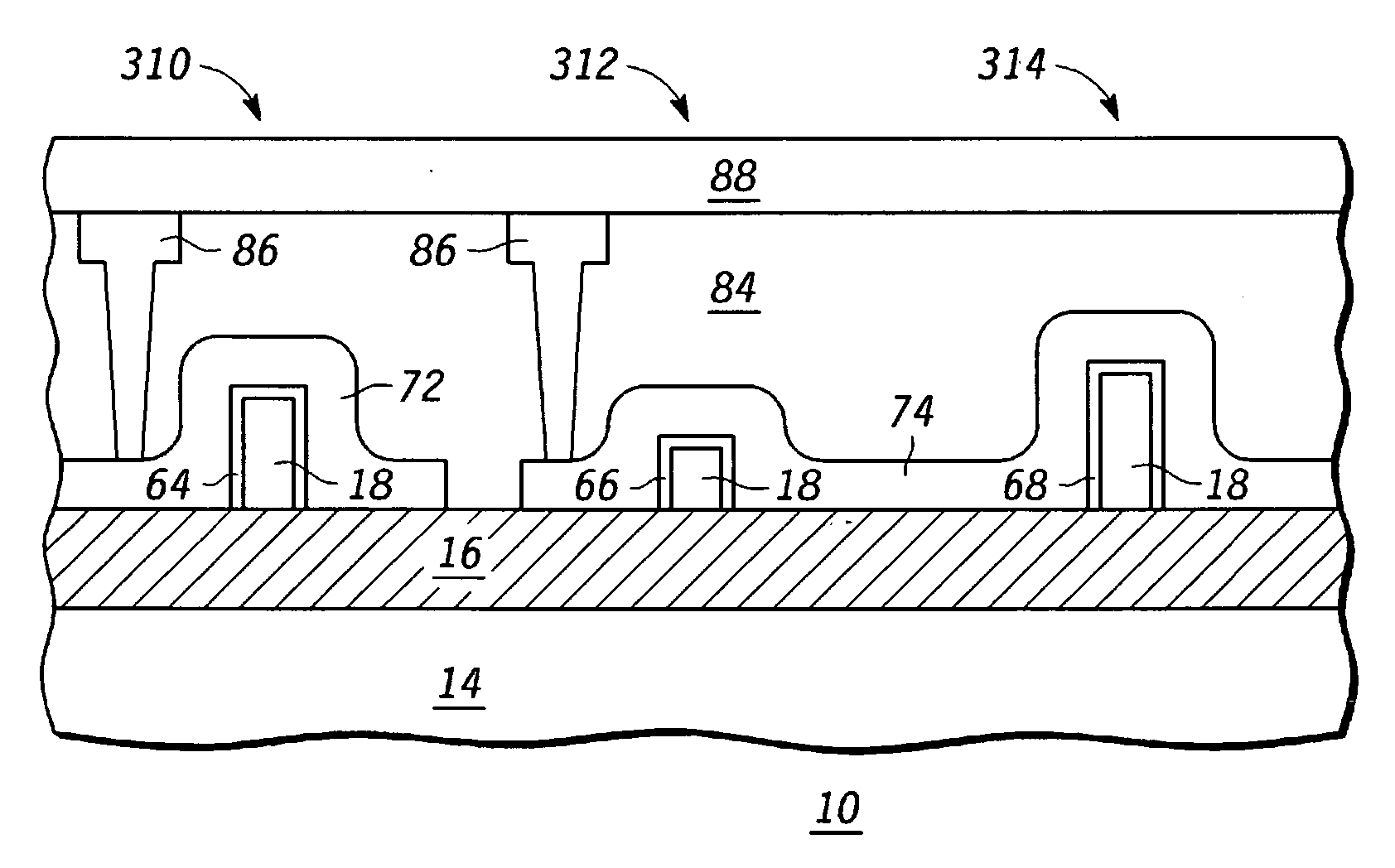
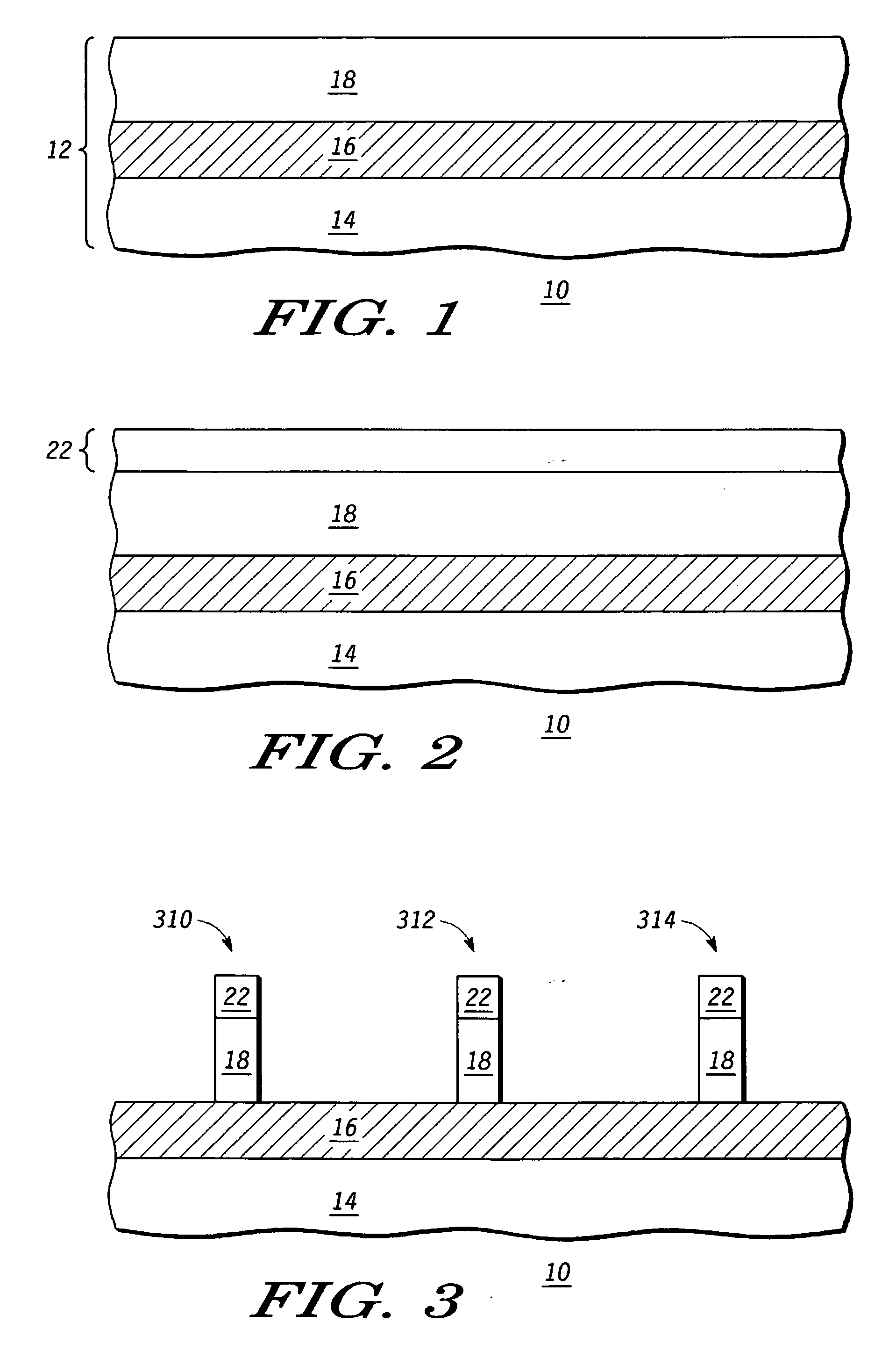
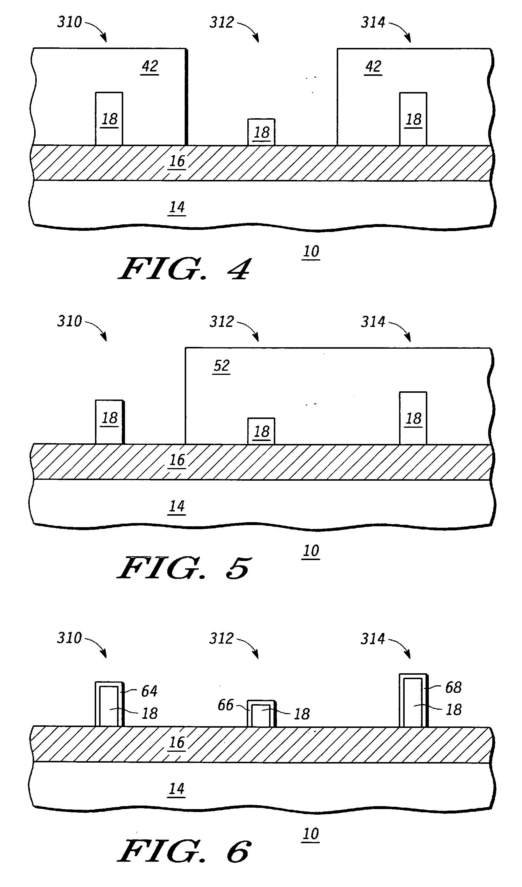
[0011] In accordance with the present disclosure, a process for forming an electronic device can include forming a semiconductor fin of a first height for a fin-type transistor structure, and removing a portion of the semiconductor fin such that the semiconductor fin is shortened to a second height. In accordance with specific embodiments a second, or a second and a third semiconductor fin portions can be formed for respective fin-type transistor structures, each semiconductor fin having a different height to provide different channel widths. In specific embodiments, semiconductor fin portions may be doped with dopants of different conductivity-types, formed with channels having different crystal orientations, or any combination thereof. Specific embodiments of the present disclosure will be better understood with reference to FIGS. 1 through 9.
[0012] Other features and advantages of the invention will be apparent from the following detailed description, and from the claims.
[0013]...
PUM
 Abstract
Description
Claims
Application Information