High linear enhancement-mode heterostructure field-effect transistor

a heterostructure, enhancement-mode technology, applied in the direction of semiconductor devices, basic electric elements, electrical apparatus, etc., can solve the problems of high transconductance speed, single saturated speed limitation of semiconductor channel layer composites, and element inability to obtain well linearity, etc., to achieve high electronic mobility, high linear e-mode heterostructure fet, and increase the range of gate voltage swing

Inactive Publication Date: 2007-08-30
FENG CHIA UNIVERSITY
View PDF2 Cites 32 Cited by
  • Summary
  • Abstract
  • Description
  • Claims
  • Application Information

AI Technical Summary

Benefits of technology

[0004] The main object of the present invention is to overcome the above problems as well as to provide a high linear E-mode heterostructure FET. The structure of the present invention is a high electronic mobility transistor comprising high linear e-mode δ-doped AlGaAs, InGaAs or InP. The structure can directly provide a complementary structure selectable for the depletion working element, and increase the range of the gate voltage swing. More, it can largely increase current driving capacity, transconductance gain, linear amplification, and high speed operation as well as directly apply in the complementary microwave active amplification semiconductor field for high potential applications in the industry.

Problems solved by technology

The channel even has high transconductance speed, but the composite of the semiconductor channel layer is limited by its single saturated speed.
Therefore, the element can not obtain a well linearity.

Method used


Image

  • High linear enhancement-mode heterostructure field-effect transistor
  • High linear enhancement-mode heterostructure field-effect transistor
  • High linear enhancement-mode heterostructure field-effect transistor

Examples


Embodiment Construction

[0017] Please refer to FIG. 1. The embodiments from the figures are only used to illustrate the present invention, not intended to limit the scope thereof.

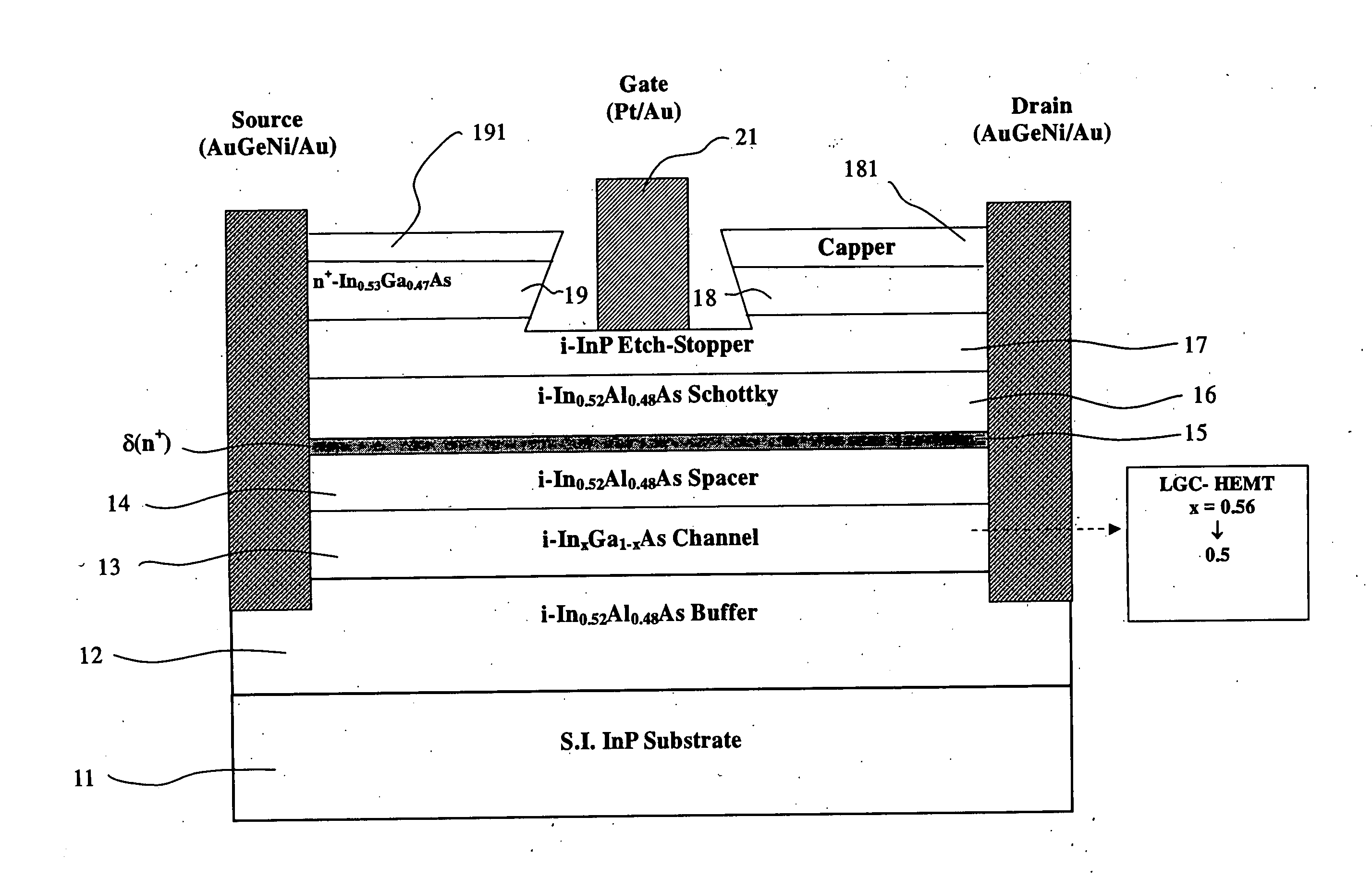
[0018]FIG. 1 is one of the preferred embodiments showing a high linear E-mode heterostructure FET. The semiconductor epitaxy structure of the transistor is grown by metal organic chemical vapor deposition (hereinafter referred to as “MOCVD”) or molecular beam epitaxy (hereinafter referred to as “MBE”). The epitaxy structure is that a In0.52Al0.48As buffer layer (12) with high energy barrier and wide band gap, a InxGa1-xAs channel layer (13) with In linear step-graded type (x is at the range between 0.56 and 0.5), a In0.52Al0.48As insulating layer (14) with high energy barrier, a Si δ-doped carrier supplier (15), a Schottky gate contact layer (16) with In0.52Al0.48As, a selective InP etch stop layer (17), and N+ drain / source ohmic contact layers (18 and 19) with high doped In0.53Ga0.47As are grown on said InP semi-insulating subst...


PUM


Abstract

The present invention relates to a high linear enhancement-mode heterostructure field-effect transistor. More, the present invention uses an InGaAs channel structure with a linear change, and integrates an adjusting effect of working region corresponding to the threshold voltage of the element. It not only directly provides a complementary structure for the conventional depletion-mode element to select, but also increases the range of the gate voltage swing. More, some important characteristics, such as current driving capacity, transconductance gain, linear amplification, and high speed operation can be largely improved. More particularly, E-mode working element has a low static power. Further, the present invention also has a high stop frequency characteristic of the high speed element from the composite semiconductor, and it can be applied to the microwave push-pull amplification circuit.

Description

BACKGROUND OF THE INVENTION [0001] The present invention relates to a high linear enhancement-mode (hereinafter referred to as “E-mode”) heterostructure field-effect transistor (hereinafter referred to as “FET”). More particularly, the high linear e-mode heterostructure field-effect structure has a channel with a linear change. By providing an e-mode field-effect element as well as using a channel with a linear change in the present invention, some important characteristics, such as high linearity, high transconductance, can be improved. Further, the structure of the present invention can be selected as a complementary working E-mode heterostructure FET for being a high linear E-mode heterostructure FET. [0002] The channel structure in conventional heterostructure field-effect transistors often has different composites in each epitaxy layer. Therefore, the channel is formed with different transconductance speed and different carrier confinements. More, a conventional channel structu...

Claims


Application Information

Patent Timeline
Patent Type & Authority Applications(United States)
IPC IPC(8): H01L31/00
CPCH01L29/7784
Inventor LEE, CHING-SUNGHSU, WEI-CHOUHUANG, JUN-CHINCHEN, CHIEN-HUNG
Owner FENG CHIA UNIVERSITY
Why Eureka
Try Eureka