Organic electroluminescence display device

a display device and electroluminescence technology, applied in the direction of discharge tube luminescnet screens, discharge tube/lamp details, electric discharge lamps, etc., can solve the problems of difficult color balance adjustment (color purity adjustment), gentle emission spectrum, etc., to increase pixel formation processes, increase white purity, and easy color purity adjustment

Active Publication Date: 2007-08-30
SAMSUNG DISPLAY CO LTD +1
View PDF2 Cites 15 Cited by
  • Summary
  • Abstract
  • Description
  • Claims
  • Application Information

AI Technical Summary

Benefits of technology

[0020]Since a pixel structure of the present invention is made by forming an organic electroluminescence layer of a white pixel at the same time as the formation of color organic electroluminescence layers that emit three primary colors of light, there is no need to increase pixel formation processes. Since the organic electroluminescence display device of the present invention serves as a light source having emission peaks of the three primary colors, color purity can be easily adjusted, and high-brightness full color images with increased white purity can be obtained.

Problems solved by technology

Since a conventional organic electroluminescence film to emit white (W) light is generally formed from a mixture of luminescent materials of two colors, an emission spectrum tends to be gentle and color balance adjustment (color purity adjustment) is difficult.

Method used


Image

  • Organic electroluminescence display device
  • Organic electroluminescence display device
  • Organic electroluminescence display device

Examples


first embodiment

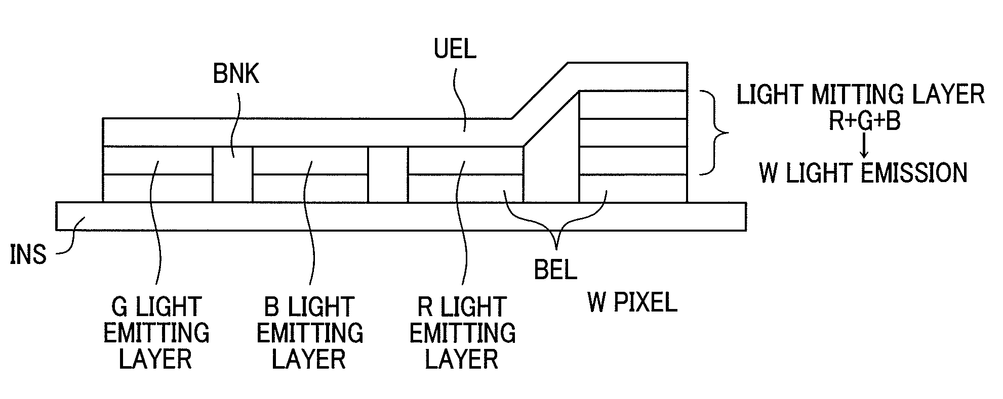
[0030]FIG. 1 is a sectional view of a full color pixel for explaining one embodiment of an organic electroluminescence display device of the R-G-B-W method of the present invention. In this drawing, a thin film transistor TFT and the like are omitted. In FIG. 1, on an insulating film INS formed on a principal surface of a glass substrate not shown, a bottom electrode BEL being a pixel electrode is formed for each of unit pixels.

[0031]A bank BNK is provided over each bottom electrode BEL. The bank BNK has the shape of a bank that surrounds a pixel concerned, for each of pixels, and an organic electroluminescence light emitting layer is charged within a region surrounded by the banks BNKs. That is, in FIG. 1, between the banks BNKs, a green light emitting layer (G light emitting layer), a blue light emitting layer (B light emitting layer), and a red light emitting layer (R light emitting layer) are provided. At the same time as the formation of these color light emitting layers, light...


PUM


Abstract

The recent invention provide an organic electroluminescence display device with color purity adjustment, particularly white purity increased, without increasing formation processes. For each of unit pixels formed on an insulating film INS formed on a principal surface of a glass substrate, a bank BNK is provided on a bottom electrode BEL being a pixel electrode. The bank BNK has the shape of a bank that surrounds a pixel concerned, for each of pixels, and an organic electroluminescence light emitting layer is charged within a region surrounded by the banks BNKs. Between the banks BNKs, a green light emitting layer (G light emitting layer), a blue light emitting layer (B light emitting layer), and a red light emitting layer (R light emitting layer) are provided. At the same time as the formation of these color light emitting layers, light emitting layers of three colors, the green light emitting layer (G light emitting layer), the blue light emitting layer (B light emitting layer), and the red light emitting layer (R light emitting layer) are stacked on a region of a white pixel to form a white light emitting layer (G+B+R). An upper electrode UEL is formed over the green light emitting layer (G light emitting layer), the blue light emitting layer (B light emitting layer), the red light emitting layer (R light emitting layer), and the white light emitting layer (G+B+R light emitting layer).

Description

CLAIM OF PRIORITY[0001]The present application claims priority from Japanese Application JP 2006-051541 filed on Feb. 28, 2006, the content of which is hereby incorporated by reference into this application.BACKGROUND OF THE INVENTION[0002]The present invention relates to organic electroluminescence display devices, and more particularly to an increase in brightness in an organic electroluminescence display device with organic electroluminescence elements of plural colors stacked on an insulating substrate that makes full color display.[0003]As display devices of flat panel type, liquid crystal displays (LCD), plasma display panels (PDP), field emission displays (FED), and organic electroluminescence displays (OLED) are commercially practical or in the stage of a study for practical use. Particularly, the organic electroluminescence display devices are greatly promising as a representative of display devices of spontaneous emission type that are thin and light in weight. The organic...

Claims


Application Information

Patent Timeline
Patent Type & Authority Applications(United States)
IPC IPC(8): H05B33/00H01J1/62
CPCH01L27/3295H01L27/3213H10K59/351H10K59/122
Inventor KAI, KAZUHIKOKINUGAWA, KIYOSHIGEITO, MASATO
Owner SAMSUNG DISPLAY CO LTD
Why Eureka
Try Eureka