Notched deposition ring

Active Publication Date: 2007-09-13
APPLIED MATERIALS INC
View PDF7 Cites 89 Cited by
  • Summary
  • Abstract
  • Description
  • Claims
  • Application Information

AI Technical Summary

Benefits of technology

[0007] Therefore, there is a ne

Problems solved by technology

For example, deposition build-up on the rings may lead to undesirable electrical bridging between the rings that adversely affect process performance, thereby requiring periodic ring replacement for cleanin

Method used


Image

  • Notched deposition ring
  • Notched deposition ring
  • Notched deposition ring

Examples


Embodiment Construction

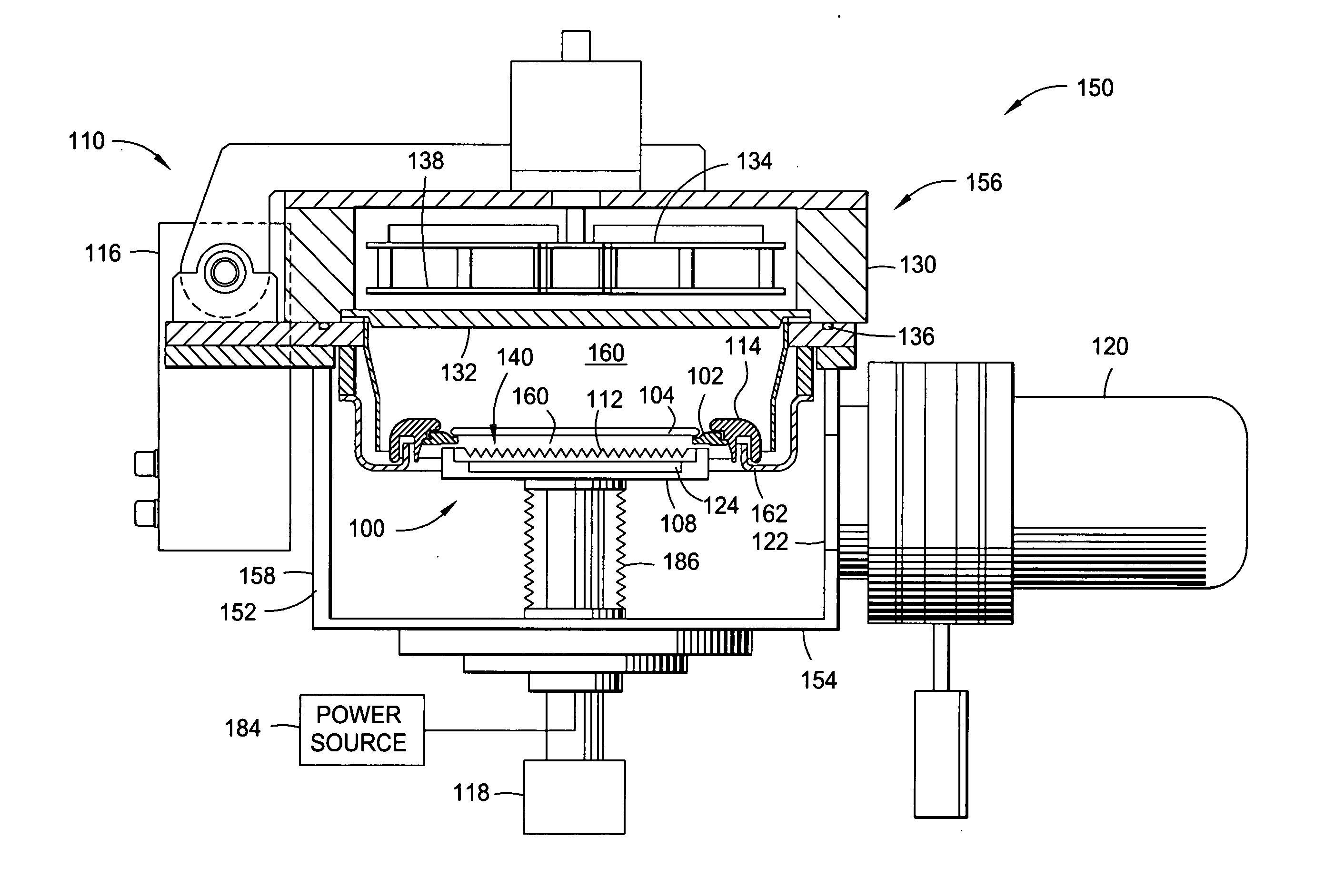
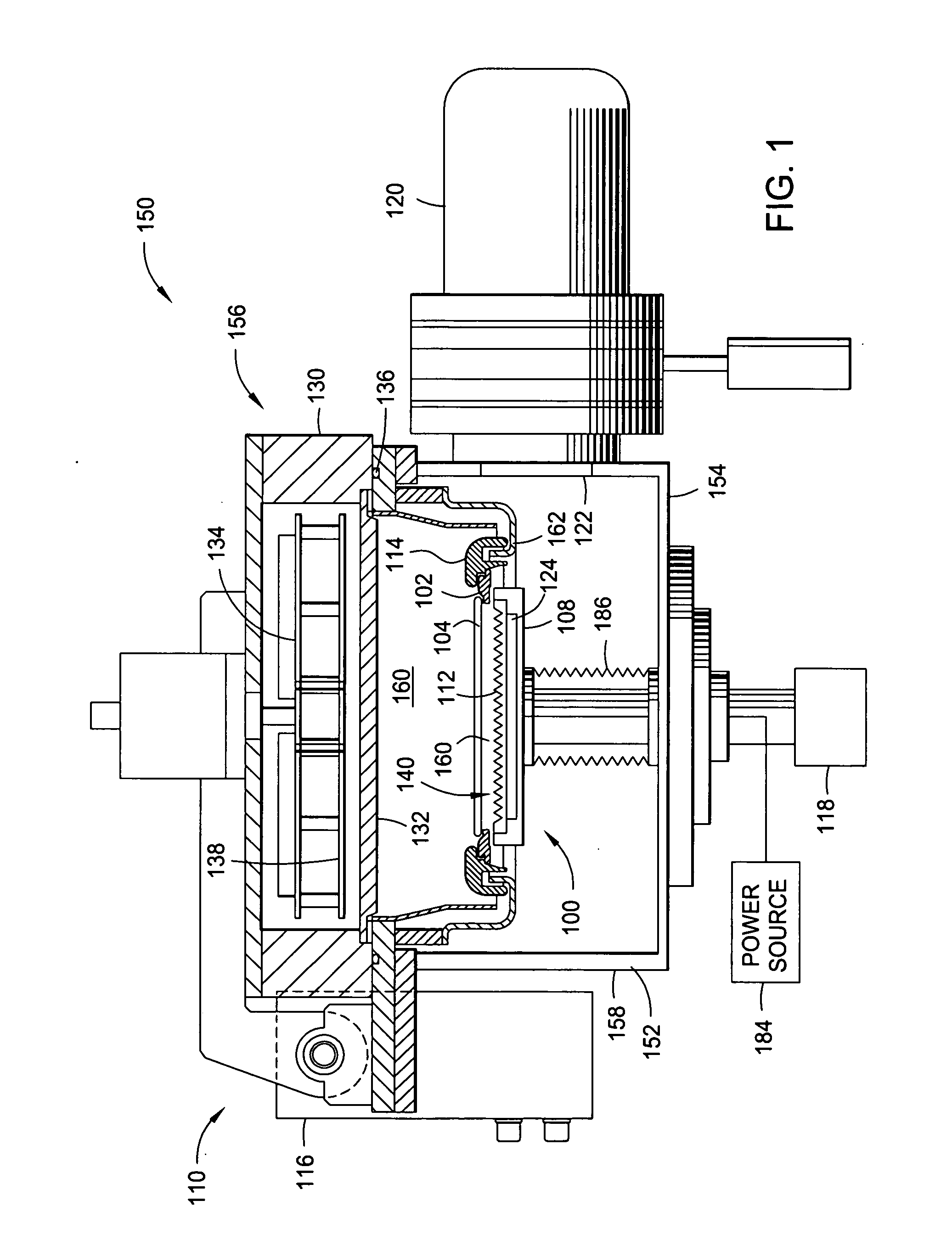
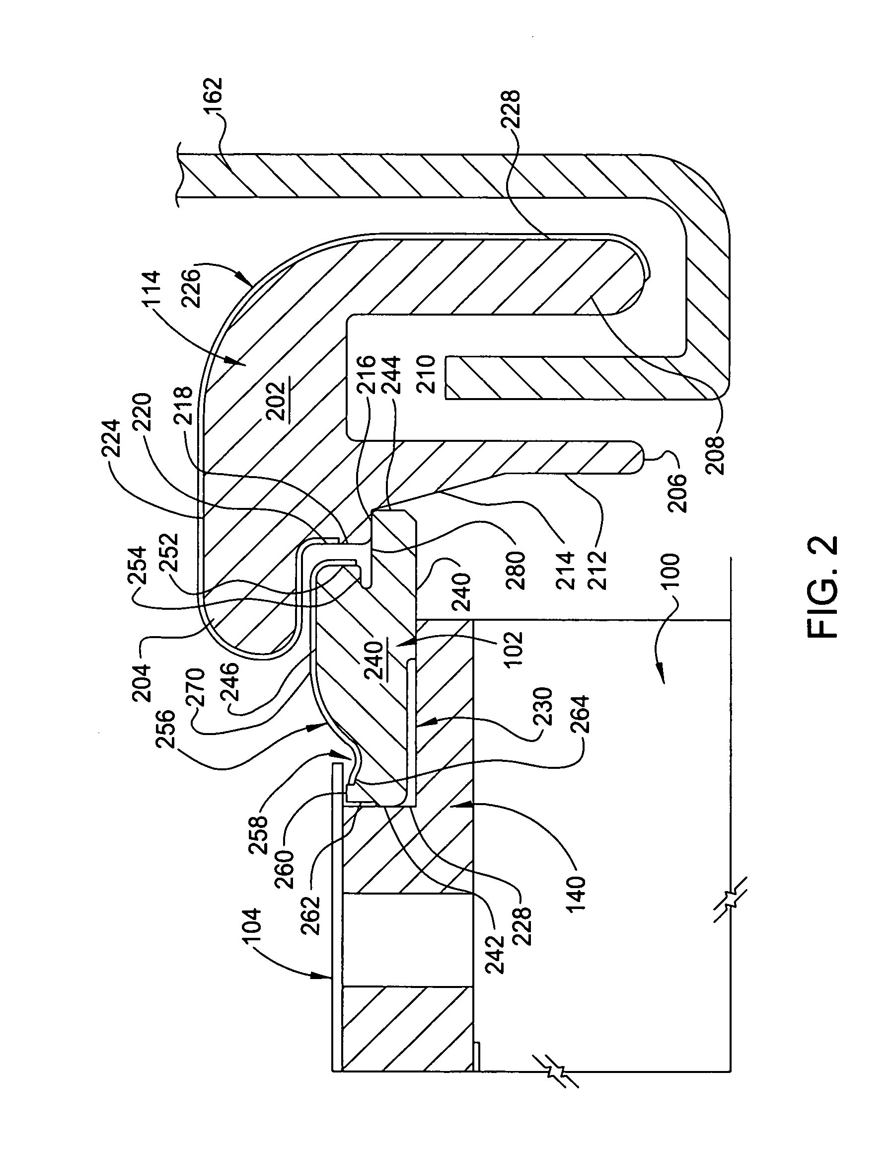
[0019] The invention generally provides a process kit for using in a semiconductor processing chamber. The process kit advantageously includes a deposition ring having at least one feature that promotes longer surface life and / or process uniformity. Although the invention is disclosed and illustrated in a physical vapor deposition (PVD) chamber, the disclosure is one of illustration, and accordingly, the invention finds utility in other semiconductor processing chambers, including chemical vapor deposition chambers, among others.

[0020]FIG. 1 depicts one embodiment of a semiconductor processing chamber 150. One example of a processing chamber that may be adapted to benefit from the invention is an IMP VECTRA™ PVD processing chamber, available from Applied Materials, Inc., of Santa Clara, Calif.

[0021] The exemplary processing chamber 150 includes a chamber body 152 having a bottom 154, lid assembly 156 and sidewalls 158 that define an evacuable interior volume 160. The chamber body ...


PUM

PropertyMeasurementUnit
Thicknessaaaaaaaaaa

Abstract

A process kit for a semiconductor processing chamber is provided. In one embodiment, a process kit includes a notched deposition ring. In another embodiment, a process kit includes a cover ring configured to engage the notched deposition ring. In another embodiment, a process kit includes an annular deposition ring body having inner, outer, upper and bottom walls. A trough is recessed into an upper surface of the body between the upper and inner walls. A recessed surface is formed on a lower surface of the body between the bottom and inner walls. A notch extends inward from the body to catch deposition material passing through a notch of the substrate being processed.

Description

BACKGROUND OF THE INVENTION [0001] 1. Field of the Invention [0002] Embodiments of the invention generally relate to process kit for a semiconductor processing chamber, and more specifically, to a notched deposition ring. [0003] 2. Description of the Related Art [0004] In deposition processes, species from a source such as a target, a gas inlet manifold and the like, may deposit on exposed internal chamber surfaces, including chamber walls, substrate pedestal assemblies, electrostatic chucks and other hardware. Process kits, such as shield assemblies, have been developed that circumscribe the electrostatic chuck within a semiconductor processing system to protect the chuck from exposure to the deposition species within the system. One shield assembly includes a removable cover ring and a deposition ring. [0005] The deposition ring rests upon a circumferential flange extending from an outer edge of the electrostatic chuck. The support surface of the chuck, upon which a substrate is r...

Claims


Application Information

Patent Timeline
IPC IPC(8): C23C14/00
CPCH01L21/68735H01J37/32495B01J3/00
Inventor MILLER, KEITH A.
Owner APPLIED MATERIALS INC
Why Eureka
Try Eureka