Ultra low pin count interface for die testing

Inactive Publication Date: 2007-09-20
INTEL CORP
View PDF5 Cites 30 Cited by
  • Summary
  • Abstract
  • Description
  • Claims
  • Application Information

AI Technical Summary

Problems solved by technology

As the complexity of Integrated Circuits (ICs) increases, the costs of testing ICs have also increased.
In general, test using BIST is significantly faster than ATE, but it has limited fault coverage.
ATE, on the other hand, achieves higher fault coverage but usually i

Method used


Image

  • Ultra low pin count interface for die testing
  • Ultra low pin count interface for die testing
  • Ultra low pin count interface for die testing

Examples


Example

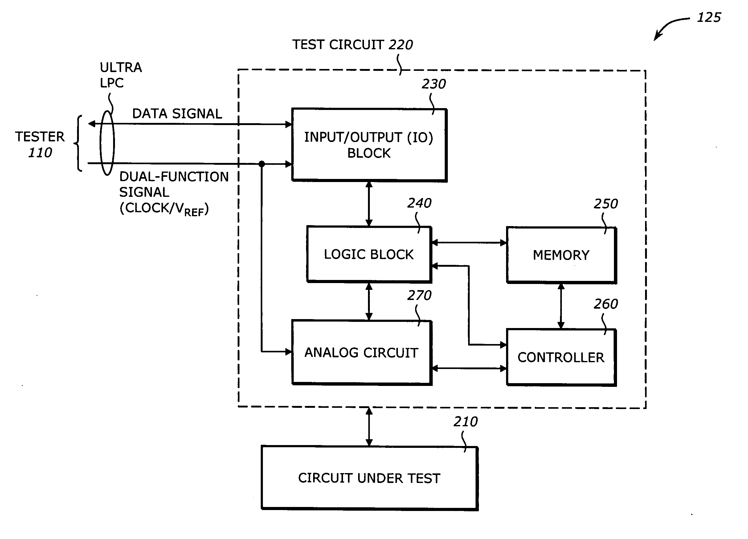
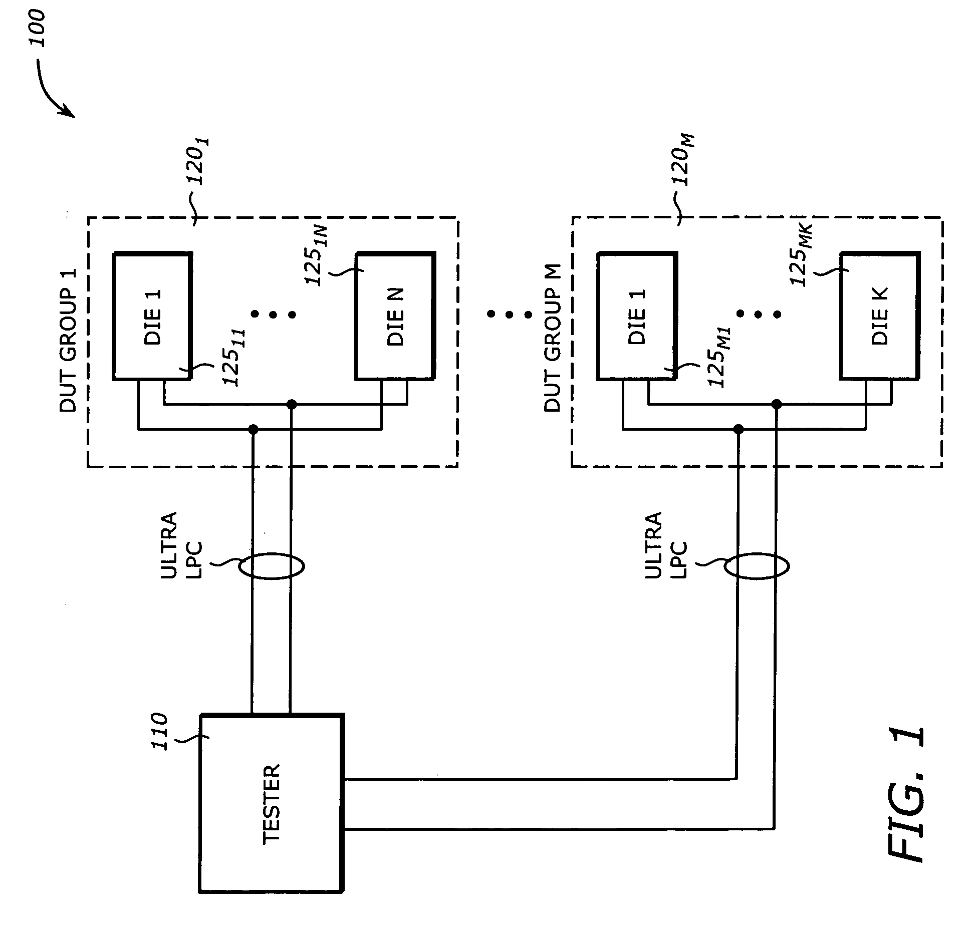
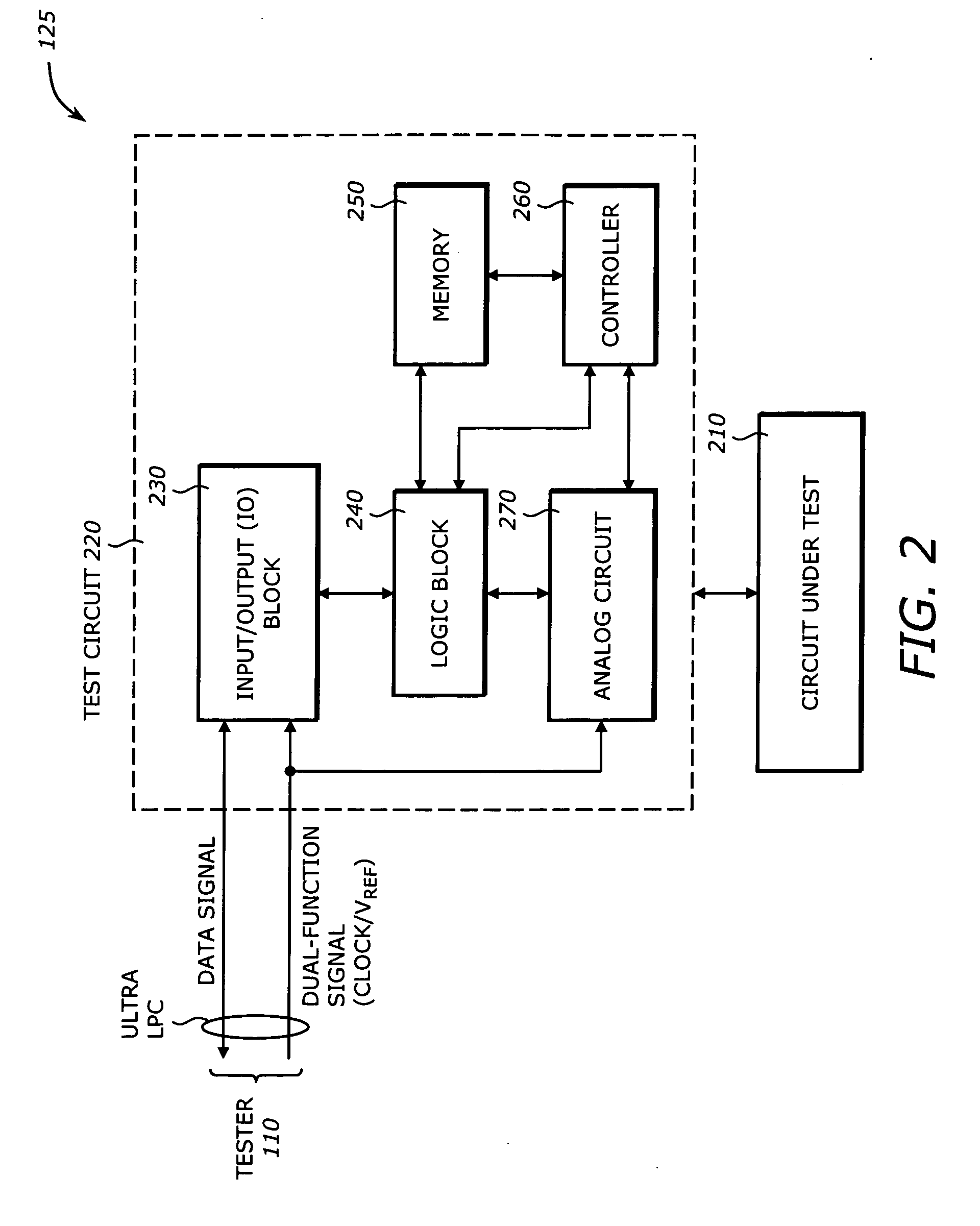
[0016] An embodiment of the present invention is a technique to test a device. An I / O block communicates with an external tester to receive test data and to send test result using first and second communication modes. A logic block parses the test data. A memory stores microcode from the parsed test data. The microcode contains a test program to test a circuit. A controller executes the test program.

[0017] In the following description, numerous specific details are set forth. However, it is understood that embodiments of the invention may be practiced without these specific details. In other instances, well-known circuits, structures, and techniques have not been shown to avoid obscuring the understanding of this description.

[0018] One embodiment of the invention may be described as a process which is usually depicted as a flowchart, a flow diagram, a structure diagram, or a block diagram. Although a flowchart may describe the operations as a sequential process, many of the operat...


PUM


Abstract

An apparatus, a method and a system to test a device. An input/output (I/O) block communicates with an external tester to receive test data and to send test result using first and second communication modes. A logic block parses the test data. A memory stores microcode from the parsed test data. The microcode contains a test program to test a circuit. A controller executes the test program.

Description

BACKGROUND [0001] 1. Field of the Invention [0002] Embodiments of the invention relate to the field of semiconductors, and more specifically, to device testing. [0003] 2. Description of Related Art [0004] As the complexity of Integrated Circuits (ICs) increases, the costs of testing ICs have also increased. To address the problem, several testing methodologies have been developed including those using Design For Test (DFT) techniques and Automated Test Equipment (ATE). DFT methodology focuses on the design of Built-in Self Test (BIST) with internal circuitry. ATE methodology focuses on developing external test controllers with interface to the DUTs. In general, test using BIST is significantly faster than ATE, but it has limited fault coverage. ATE, on the other hand, achieves higher fault coverage but usually incurs longer test time. [0005] One major problem in testing ICs is the Input / Output (I / O) communication between the external tester (e.g., ATE) and the Device Under Test (DUT...

Claims


Application Information

Patent Timeline
IPC IPC(8): G01R31/26
CPCG01R31/3167G01R31/3172G11C2029/5602G11C2029/2602G11C29/56
Inventor GUPTA, SUNILLINDE, REEDFACKENTHAL, RICH
Owner INTEL CORP
Why Eureka
Try Eureka