Uniform emission LED package

a technology of led packaging and led components, applied in the field of led packaging and led packaging methods, can solve the problems of complicated control electronics of devices, degraded long-term wavelength and stability of these devices, and problems such as making problems wors

Active Publication Date: 2007-10-04
CREELED INC
View PDF99 Cites 67 Cited by
  • Summary
  • Abstract
  • Description
  • Claims
  • Application Information

AI Technical Summary

Problems solved by technology

In addition, different colors of light are often generated from different types of LEDs which can require complex fabrication to combine in one device.
The resulting devices can also require complicated control electronics since the different diode types can require different control voltages.
Long term wavelength and stability of these devices is also degraded by the different aging behavior of the different LEDs.
This packaging,

Method used


Image

  • Uniform emission LED package
  • Uniform emission LED package
  • Uniform emission LED package

Examples


Embodiment Construction

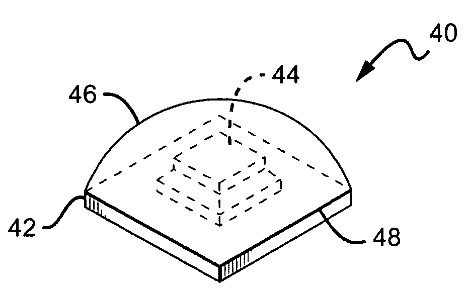
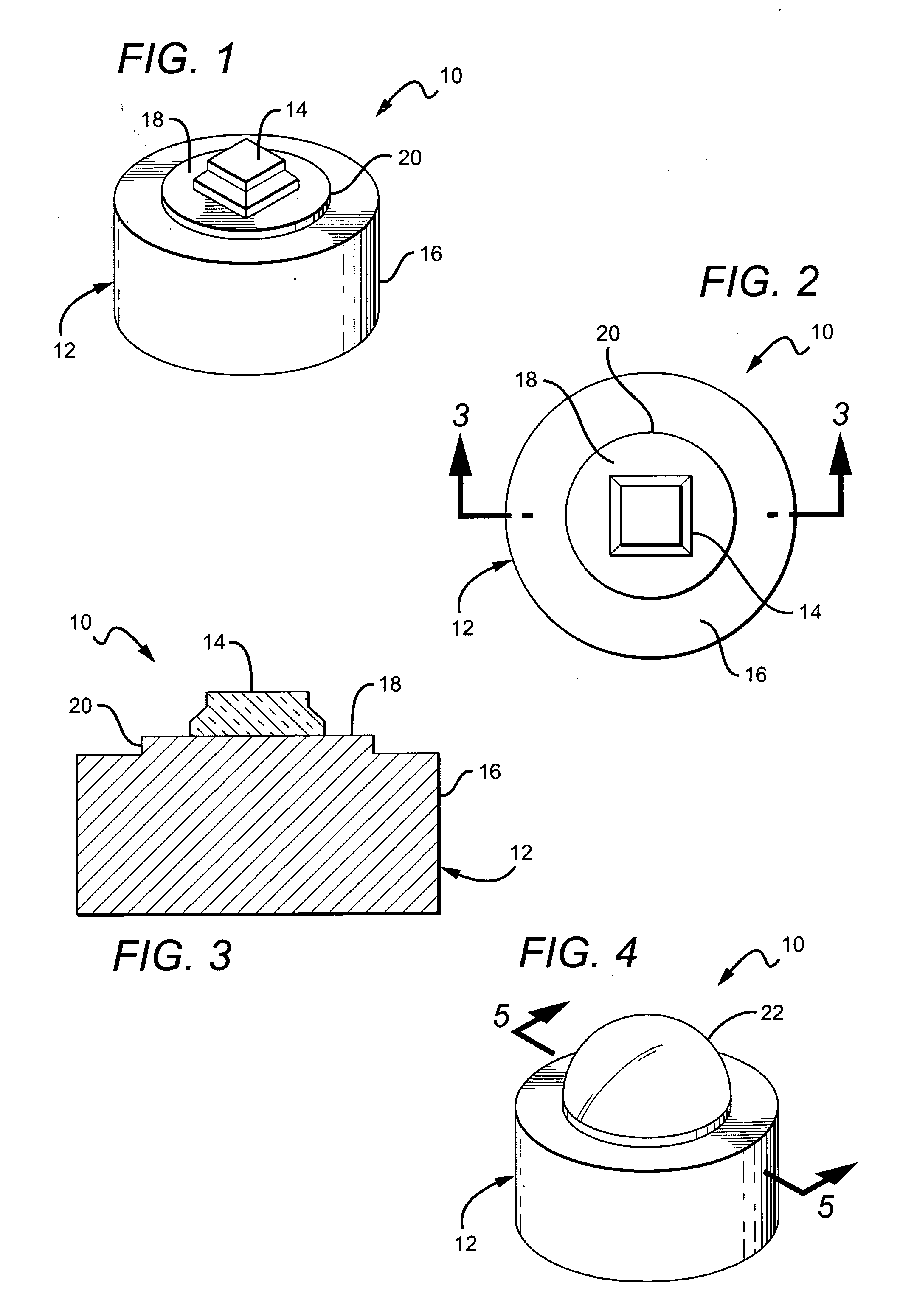
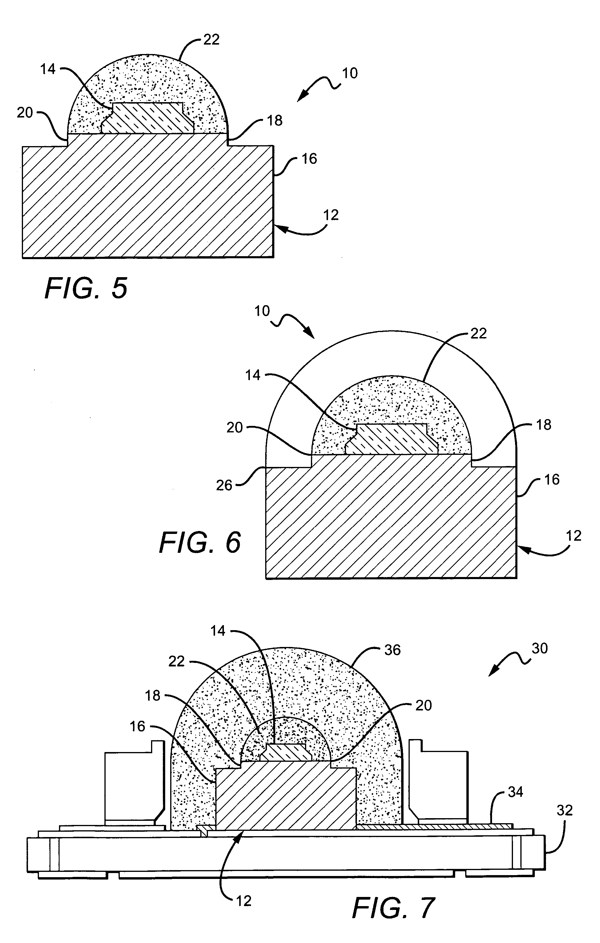
[0032] The present invention provides LED packages and methods for fabricating LED packages utilizing a simple, inexpensive dispense process to create a compact, free standing, hemispherical phosphor converter layer surrounding the LED. The phosphor particles in this layer reside close to the chip such that both converted and unconverted light are produced near the same “point in space.” This allows the LED package to produce substantially the same ratio of converted and LED light at different viewing angles, thereby producing substantially uniform light at different viewing angles.

[0033] The present invention is described herein with reference to certain embodiments but it is understood that the invention can be embodied in many different forms and should not be construed as limited to the embodiments set forth herein. It is also understood that when an element such as a layer, region or substrate is referred to as being “on” another element, it can be directly on the other elemen...


PUM


Abstract

An emitter package comprising a light emitting diode (LED) mounted to the surface of a submount with the surface having a first meniscus forming feature around the LED. A matrix encapsulant is included on the surface and covering the LED. The outer edge of the matrix encapsulant adjacent the surface is defined by the meniscus forming feature and the encapsulant forms a substantially dome-shaped covering over said LED. A method for manufacturing an LED package by providing a body with a surface having a first meniscus holding feature. An LED is mounted to the surface with the meniscus holding feature around the LED. A liquid matrix encapsulant is introduced over the LED and the surface, the first meniscus holding feature holding the liquid matrix encapsulant in a dome-shape over the LED. The matrix encapsulant is then cured.

Description

BACKGROUND OF THE INVENTION [0001] 1. Field of the Invention [0002] This invention relates to semiconductor light emitting diodes (LEDs) and more particularly to LED packages and LED packaging methods. [0003] 2. Description of the Related Art [0004] Light emitting diodes (LEDs) are solid state devices that convert electric energy to light, and generally comprise one or more active layers of semiconductor material sandwiched between oppositely doped layers. When a bias is applied across the doped layers, holes and electrons are injected into the active layer where they recombine to generate light. Light is emitted omnidirectionally from the active layer and from all surfaces of the LED. The useful light is generally emitted in the direction of the LED's top surface, which is usually p-type. [0005] Conventional LEDs cannot generate white light from their active layers. One way to produce white light from conventional LEDs is to combine different colors from different LEDs. For example...

Claims


Application Information

Patent Timeline
IPC IPC(8): H01L33/00H01L21/00H01L33/48H01L33/50
CPCH01L33/486H01L33/505H01L33/507H01L2924/0002H01L2924/00H01L33/54H01L33/58H01L2933/0033H01L2933/005
Inventor NEGLEY, GERALDLEUNG, MICHAELBECERRA, MARYANNETARSA, ERICANDREWS, PETER
Owner CREELED INC
Why Eureka
Try Eureka