Solid-state imaging apparatus and method for driving solid-state imaging device

a solid-state imaging and imaging apparatus technology, applied in the direction of radioation control devices, television system scanning details, television systems, etc., can solve the problems of poor image quality, inability to combine, jagged edges, etc., and achieve the effect of suppressing image quality deficiencies

Inactive Publication Date: 2007-10-11
PANASONIC CORP
View PDF6 Cites 2 Cited by
  • Summary
  • Abstract
  • Description
  • Claims
  • Application Information

AI Technical Summary

Benefits of technology

[0011]With the foregoing conventional problems in mind, it is an object of the present invention to provide a solid-state imaging apparatus that can suppress image quality deficiencies due to transfer degradation and mix a dummy signal with a signal charge in the case where a dummy transfer stage is formed for transfer.

Problems solved by technology

However, it would not be possible to combine the configuration described in JP 9(1997)-18792 A capable of reducing the number of pixels in the vertical direction with that described in JP 2004-180284 A capable of reducing the number of pixels in the horizontal direction.
However, in this case, there is a problem that a smear occurring when capturing an image of a radiant with too much light quantity has a jagged edge, though a smear naturally has a linear edge.
Further, even in the case where no smear occurs, if a transfer leakage from the vertical transfer stage that is transferring a signal charge causes the signal charge to leak into the dummy transfer stage during transfer through the vertical transfer stages, the leaking signal charge sometimes is mixed with the signal charge in another column in the horizontal transfer portion, which may result in poor image quality due to transfer degradation.

Method used


Image

  • Solid-state imaging apparatus and method for driving solid-state imaging device
  • Solid-state imaging apparatus and method for driving solid-state imaging device
  • Solid-state imaging apparatus and method for driving solid-state imaging device

Examples


Embodiment Construction

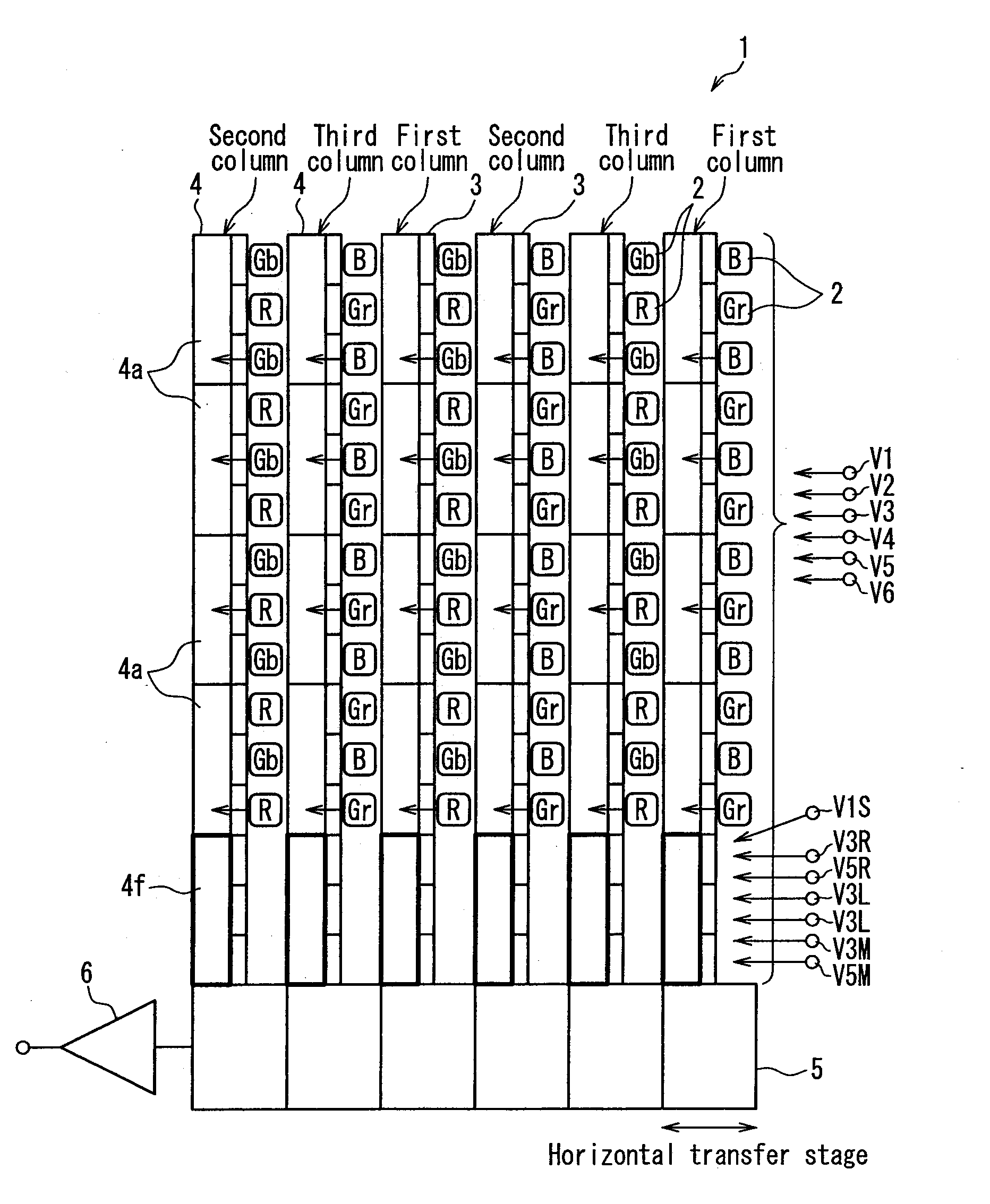
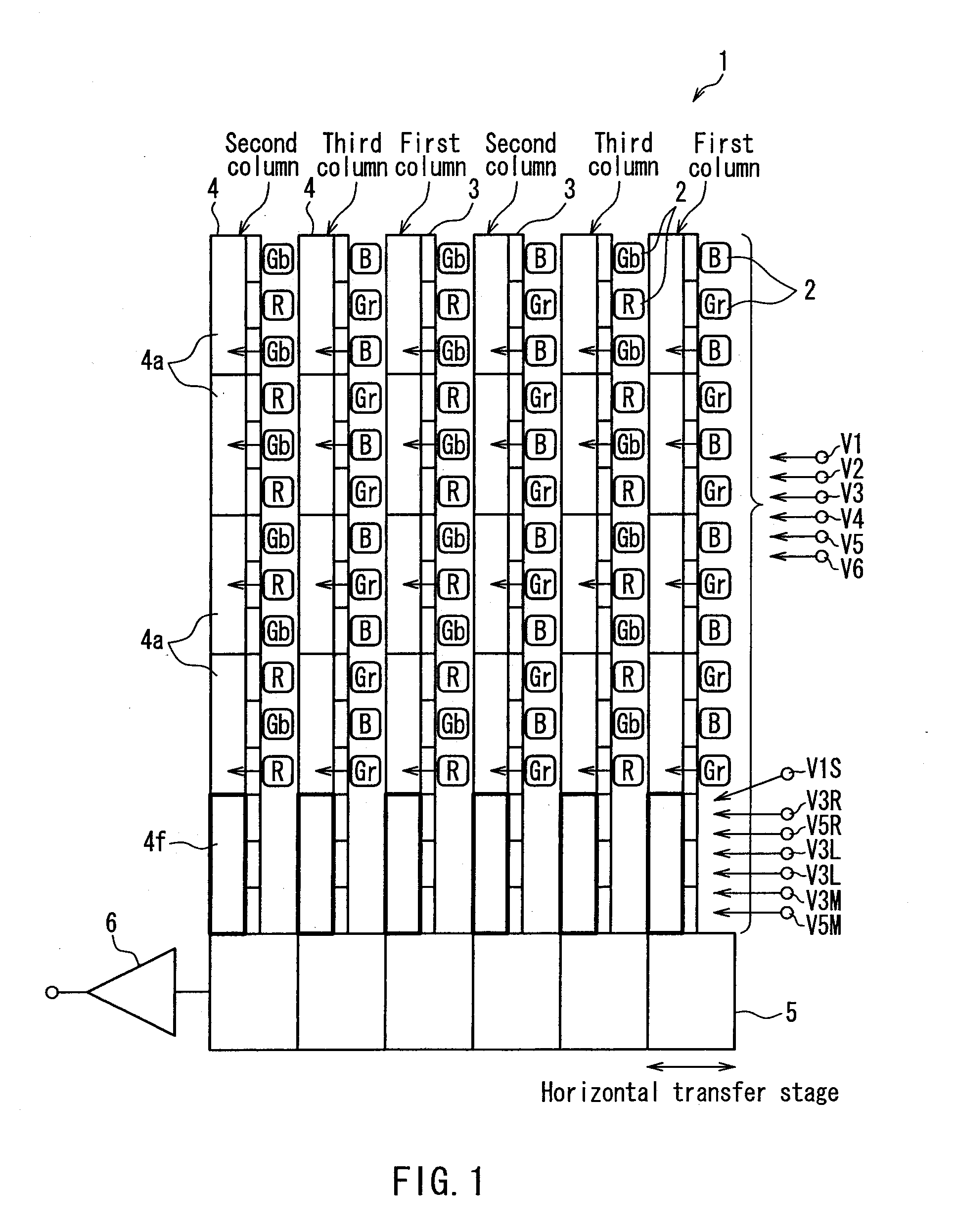
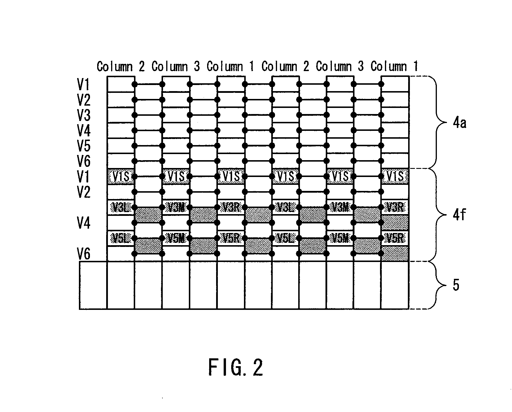
[0024]With the solid-state imaging apparatus or the method for driving a solid-state imaging device according to the present invention, the transfer electrodes at the vertical last stage include at least two phases of independent transfer electrodes that are independent of the other vertical transfer stages, and the independent transfer electrodes have identical configurations repeated in a unit of n columns, and are constituted so as to be in common among each column in the unit of n columns and independent of the independent transfer electrodes belonging to the other columns in the unit of n columns. A signal transfer stage from which the signal charge is read out and a dummy transfer stage from which the signal charge is not read out are formed alternately, and the signal charge at the signal transfer stage and a dummy signal at the following dummy transfer stage are mixed together at the vertical last stage and then transferred to the horizontal transfer portion. By operating th...


PUM


Abstract

Vertical transfer portions for transferring signal charges from photoelectric conversion portions in a vertical direction and a horizontal transfer portion for transferring them in a horizontal direction are provided, and each of a plurality of vertical transfer stages constituting the vertical transfer portion is provided with a plurality of phases of transfer electrodes. The transfer electrodes at a vertical last stage include independent transfer electrodes (V3R, V5R) for at least two phases, that are independent of the other vertical transfer stages, have identical configurations repeated in a unit of n columns, and are in common among corresponding columns in a plurality of the units of n columns and independent of the independent transfer electrodes belonging to the other columns in the unit of n columns. A signal transfer stage from which the signal charge is read out and a dummy transfer stage from which the signal charge is not read out are formed alternately, the signal charge at the signal transfer stage and a dummy signal at the following dummy transfer stage are mixed together at the vertical last stage and then transferred to the horizontal transfer portion. In the case where a dummy transfer stage is formed for transfer, it is possible to suppress transfer degradation and mix a dummy signal with a signal charge.

Description

BACKGROUND OF THE INVENTION[0001]1. Field of the Invention[0002]The present invention relates to a solid-state imaging apparatus and a method for driving a solid-state imaging device, in which light received by a plurality of two-dimensionally arranged photoelectric conversion portions is converted into electric signals and outputted as image signals. In particular, the present invention relates to a solid-state imaging apparatus and a method for driving a solid-state imaging device, in which the image signals can be outputted at a high frame rate.[0003]2. Description of Related Art[0004]Known solid-state imaging devices, which convert light received by individual pixels into electric signals and output them as image signals, include those using CCDs (charge-coupled devices). Also, digital still cameras utilizing such solid-state imaging devices have been widespread. In recent years, with an increase in the density of pixels in the solid-state imaging devices, the digital still came...

Claims


Application Information

Patent Timeline
Patent Type & Authority Applications(United States)
IPC IPC(8): H04N5/335H01L27/148H04N5/341H04N5/359H04N5/3728H04N5/376H04N9/07
CPCH01L27/14603H01L27/14621H01L27/14843H04N9/045H04N5/335H04N5/3595H04N5/37213H04N3/155H04N25/625H04N25/713H04N25/70H04N23/84H04N25/134H04N25/00
Inventor KATO, YOSHIAKI
Owner PANASONIC CORP
Why Eureka
Try Eureka