

Semiconductor device package with base features to reduce leakage
a technology for semiconductor devices and base features, applied in semiconductor devices, semiconductor/solid-state device details, electrical devices, etc., can solve problems such as encapsulant leakage at the plastic, deterioration of the interface between the different parts of the package, and non-hermetic plastic packages fabricated in this or similar fashion
- Summary
- Abstract
- Description
- Claims
- Application Information
AI Technical Summary
Benefits of technology
Problems solved by technology
Method used
Image

Examples
example
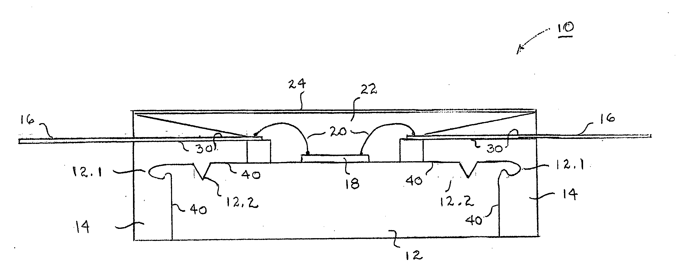
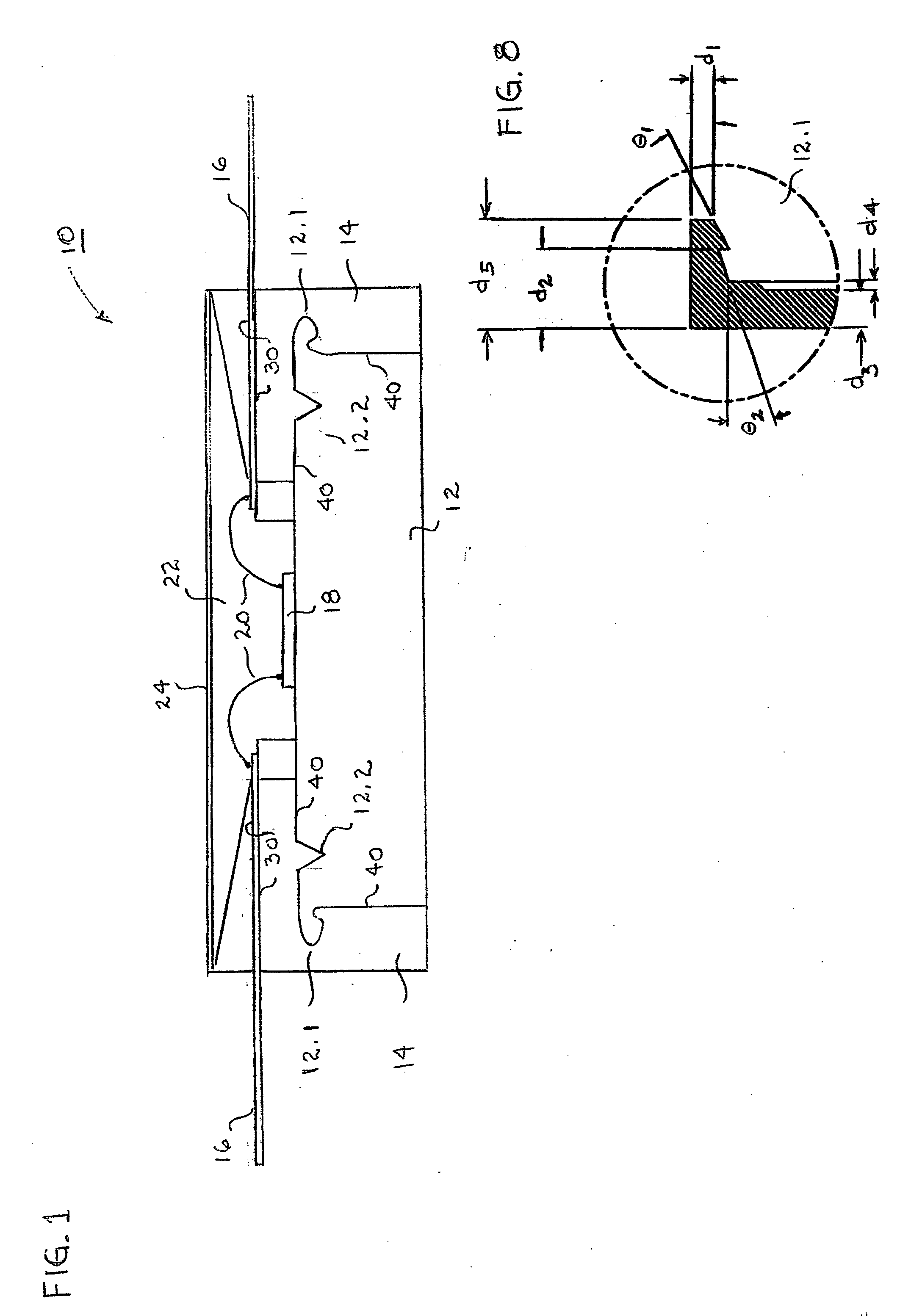
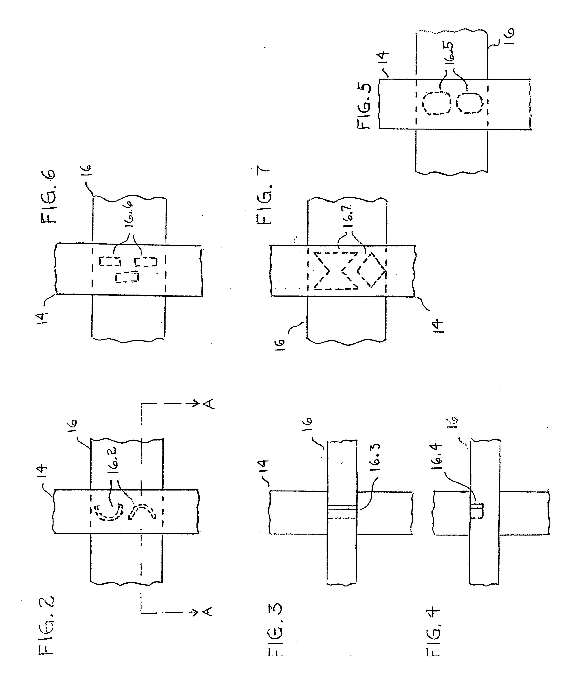
[0031] This example describes the fabrication of a package for RFLDMOS (i.e., radio frequency, laterally diffused, metal-oxide-semiconductor) ICs, in accordance with one embodiment of our invention. Various materials, dimensions and operating conditions are provided by way of illustration only and, unless otherwise expressly stated, are not intended to limit the scope of the invention. This type of package illustratively contains six chips: two chips that function as active ICs (i.e., high power RFLDMOS transistors) and four that function as passive ICs (i.e., capacitors).
[0032] The container 12 had overall dimensions of 810 mils in length, 385 mils in width, and 99 mils in height. The sidewalls 14 and lid 24 were made of a liquid crystal polymer (LCP) material (e.g., Ticona Vectra S-135). The sidewalls were 72.5 mils thick in the region where the lead frame extended through the sidewalls, whereas the lid 24 had overall dimensions of 810 mils in length, 384 mils in width, and 43 mi...
PUM
 Abstract
Description
Claims
Application Information